Absolute maximum ratings, Electrical characteristics – Rainbow Electronics MAX913 User Manual
Page 2
MAX912/MAX913
Single/Dual, Ultra-Fast, Low-Power,
Precision TTL Comparators
2
_______________________________________________________________________________________
ABSOLUTE MAXIMUM RATINGS
Positive Supply Voltage............................................................7V
Negative Supply Voltage ........................................................-7V
Differential Input Voltage .....................................................±15V
Input Voltage (Referred to V-)..................................- 0.3V to 15V
Latch Pin Voltage .............................................Equal to Supplies
Continuous Output Current...............................................±20mA
Continuous Power Dissipation (T
A
= +70°C)
8-Pin Plastic DIP (derate 9.09mW/°C above +70°C) ...727mW
8-Pin SO (derate 5.88mW/°C above +70°C)................471mW
8-Pin CERDIP (derate 8.00mW/°C above +70°C)........640mW
16-Pin Plastic DIP (derate 10.53mW/°C above +70°C)...842mW
16-Pin Narrow SO (derate 8.70mW/°C above +70°C) ...696mW
16-Pin CERDIP (derate 10.00mW/°C above +70°C)....800mW
Operating Temperature Ranges:
MAX91_ C_ _ ......................................................0°C to +70°C
MAX91_ E_ _....................................................-40°C to +85°C
MAX91_ MJ_ .................................................-55°C to +125°C
Storage Temperature Range .............................-65°C to +150°C
Lead Temperature (soldering, 10sec) .............................+300°C
Stresses beyond those listed under “Absolute Maximum Ratings” may cause permanent damage to the device. These are stress ratings only, and functional
operation of the device at these or any other conditions beyond those indicated in the operational sections of the specifications is not implied. Exposure to
absolute maximum rating conditions for extended periods may affect device reliability.
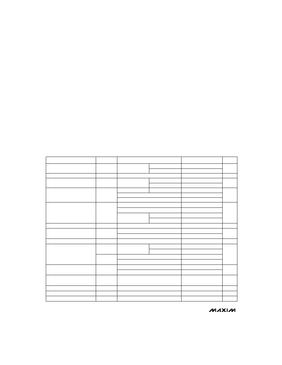
PARAMETER
R
S
≤
100
Ω
SYMBOL
MIN
TYP
MAX
T
A
= T
MIN
to T
MAX
UNITS
T
A
= +25°C
3
T
A
= T
MIN
to T
MAX
Offset Drift
TCV
OS
2
µV/°C
Input Offset Current (Note 1)
I
OS
0.3
0.5
µA
T
A
= +25°C
0.8
T
A
= +25°C
Input Bias Current
I
B
3
5
µA
C, E temp. ranges
8
M temp. range
10
CONDITIONS
Input Offset Voltage (Note 1)
V
OS
0.8
2
mV
Single +5V
C, E temp. ranges
Power-Supply Rejection Ratio
PSRR
M temp. range
Positive supply: 4.5V
≤
V+
≤
5.5V
60
85
M temp. range
-5.0
+3.5
-5.0V
≤
V
CM
≤
+3.5V
dB
I
OUT
= 1mA
V
OL
-0.2
+3.5
Negative supply: -2V
≥
V-
≥
-7V
Common-Mode Rejection Ratio
CMRR
80
100
0
+3.5
dB
C, E temp. ranges
I
OUT
= 10mA
80
110
Small-Signal Voltage Gain
A
V
1V
≤
V
Q
≤
2V, T
A
= +25°C
1500
3500
V/V
Output Voltage
V
OH
V+
≥
4.5V
2.7
3.4
V
2.4
3.0
I
SINK
= 4mA
0.3
0.5
T
A
= +25°C, I
SINK
= 10mA
0.4
Input Voltage Range
V
CM
-5.2
+3.5
V
ELECTRICAL CHARACTERISTICS
(V+ = +5V, V- = -5V, V
Q
= 1.4V, V
LE
= 0V, T
A
= T
MIN
to T
MAX
, unless otherwise noted. Typical values are at T
A
= +25°C.)
12
C, E temp. ranges
6
10
Positive Supply Current Per
Comparator
I+
M temp. range
12
mA
Latch-Pin High Input Voltage
V
IH
I-
0.4
2
mA
2.0
V
Latch-Pin Current
I
IL
V
LE
= 0V
Latch-Pin Low Input Voltage
V
IL
0.8
V
-20
µA
Negative Supply Current Per
Comparator