Detailed description, Applications information – Rainbow Electronics MAX913 User Manual
Page 7
_______________Detailed Description
The MAX913 (single) and MAX912 (dual) high-speed
comparators have a unique design that prevents oscil-
lation when the comparator is in its linear region. No
minimum input slew rate is required.
Many high-speed comparators oscillate in the linear
region, as shown in the
Typical Operating
Characteristics’ industry-standard 686 response graph.
One way to overcome this oscillation is to sample the
output after it has passed through the unstable region.
Another practical solution is to add hysteresis. Either
solution results in a loss of resolution and bandwidth.
Because the MAX912/MAX913 do not need hysteresis,
they offer high resolution to all signals—including low-
frequency signals.
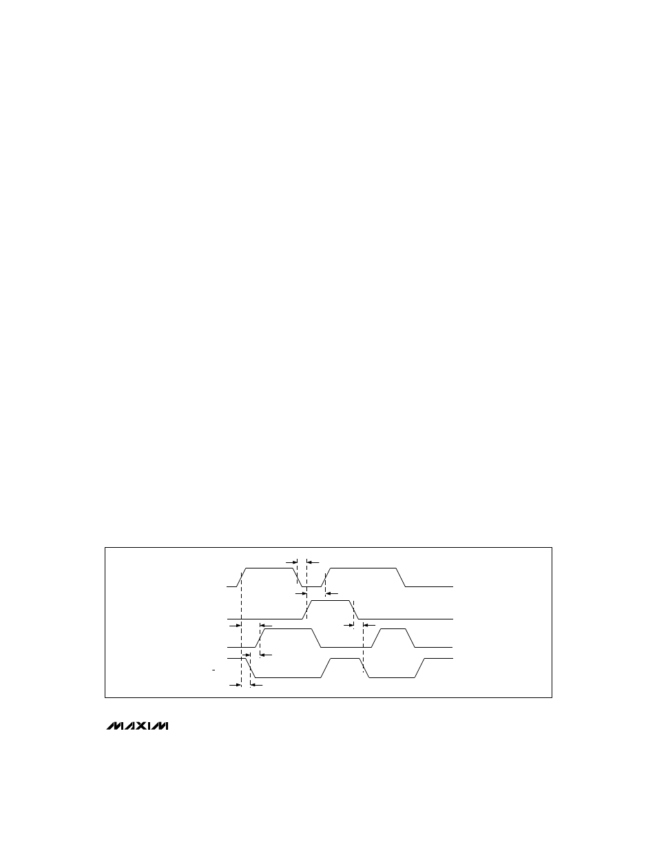
The MAX912/MAX913 provide a TTL-compatible latch
function that holds the comparator output state (Figure 1).
As long as Latch Enable (LE) is high or floating, the input
signal has no effect on the output state. With LE low, the
outputs are controlled by the input differential voltage and
the latch is transparent.
Input Amplifier
A comparator can be thought of as having two sec-
tions: an input amplifier and a logic interface. The
MAX912/MAX913’s input amplifier is fully differential,
with input offset voltage trimmed to below 2.0mV at
+25°C. Input common-mode range extends from
200mV
below
the negative supply rail to 1.5V below the
positive power supply. The total common-mode range
is 8.7V when operating from ±5VDC supplies.
The MAX912/MAX913’s amplifier has no built-in hys-
teresis. For highest accuracy, do not add hysteresis.
Figure 2 shows how hysteresis degrades resolution.
Resolution
A comparator’s ability to resolve small signal differ-
ences—its resolution—is affected by various factors.
As with most amplifiers, the most significant factors are
the input offset voltage (V
OS
) and the common-mode
and power-supply rejection ratios (CMRR, PSRR). If
source impedance is high, input offset current can be
significant. If source impedance is unbalanced, the
input bias current can introduce another error.
For high-speed comparators, an additional factor in reso-
lution is the comparator’s stability in its linear region. Many
high-speed comparators are useless in their linear region
because they oscillate. This makes the differential input
voltage region around 0V unusable, as does a high V
OS.
Hysteresis does not cure the problem, but acts to keep
the input away from its linear range (Figure 2).
The MAX912/MAX913 do not oscillate in the linear region,
which greatly enhances the comparator’s resolution.
__________Applications Information
Power Supplies and Bypassing
The MAX912/MAX913 are tested with ±5V power sup-
plies that provide an input common-mode range (V
CM
)
of 8.7V (-5.2V to +3.5V). Operation from a single +5V
supply provides a common-mode input range of 3.7V
(-0.2V to +3.5V). Connect V- to GND for single-supply
operation. The MAX912/MAX913 will operate from a
minimum single-supply voltage of +4.5V.
The V+ supply provides power to both the analog input
stage and digital output circuits, whereas the V- supply
only powers the analog section. Bypass V+ and V- to
ground with 0.1µF to 1.0µF ceramic capacitors in parallel
with 10µF or greater tantalum capacitors. Connect the
ceramic capacitors very close to the MAX912/MAX913’s
MAX912/MAX913
Single/Dual, Ultra-Fast, Low-Power,
Precision TTL Comparators
_______________________________________________________________________________________
7
t
SU
t
H
t
PD+
∆
t
PD
t
PD-
t
LPDR
Q
Q
V
IN
(DIFFERENTIAL)
LATCH
ENABLE (LE)
Figure 1. Timing Diagram