Typical operating characteristics, Electrical characteristics (continued) – Rainbow Electronics MAX913 User Manual
Page 3
MAX912/MAX913
Single/Dual, Ultra-Fast, Low-Power,
Precision TTL Comparators
_______________________________________________________________________________________
3
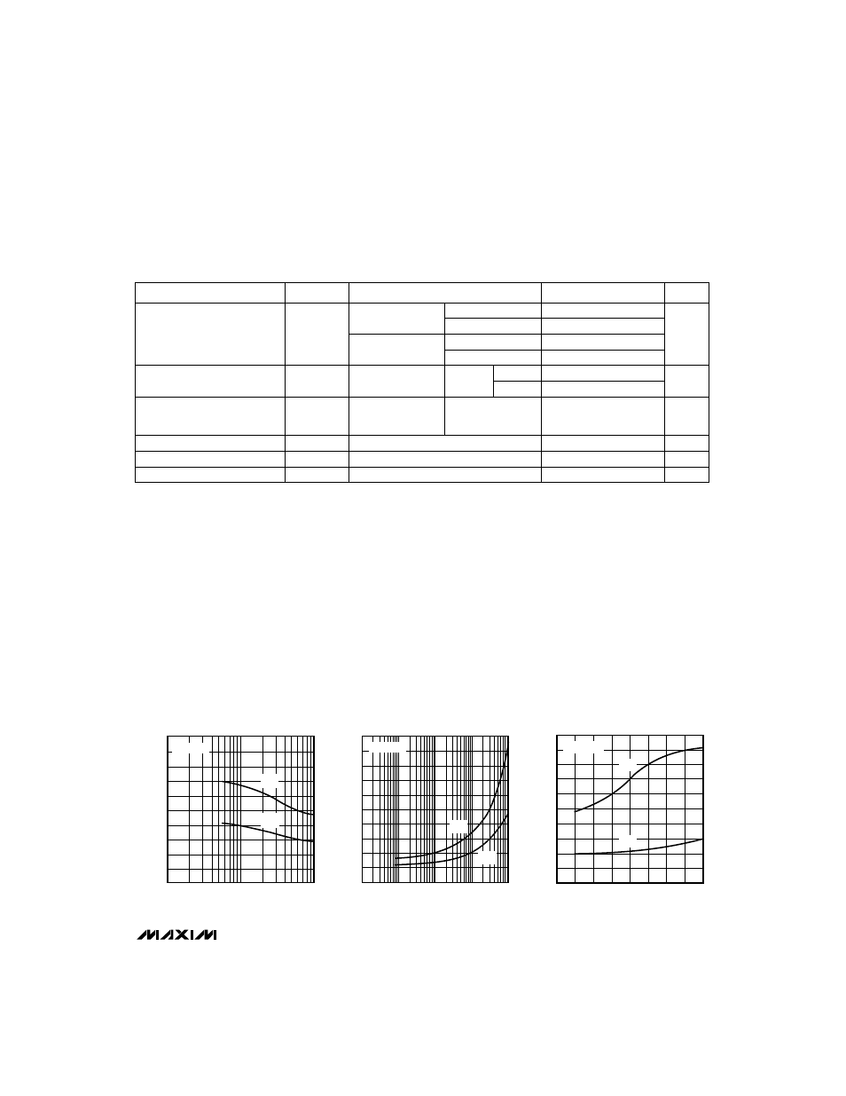
ELECTRICAL CHARACTERISTICS (continued)
(V+ = +5V, V- = -5V, V
Q
= 1.4V, V
LE
= 0V, T
A
= T
MIN
to T
MAX
, unless otherwise noted).
T
A
= +25°C
T
A
= T
MIN
to T
MAX
∆
V
IN
= 100mV,
V
OD
= 20mV
9
12
T
A
= +25°C
Propagation Delay (Note 2)
t
PD+
, t
PD-
∆
V
IN
= 100mV,
V
OD
= 5mV
10
14
ns
16
15
T
A
= T
MIN
to T
MAX
Note 1:
Input Offset Voltage (V
OS
) is defined as the average of the two input offset voltages, measured by forcing first one output,
then the other to 1.4V. Input Offset Current (I
OS
) is defined the same way.
Note 2:
Propagation Delay (t
PD
) and Differential Propagation Delay (
∆
t
PD
) cannot be measured in automatic handling equipment
with low input overdrive values. The MAX912/MAX913 are sample tested to 0.1% AQL with a 1V step and 500mV overdrive
at +25°C only. Correlation tests show that t
PD
and
∆
t
PD
can be guaranteed with this test, if additional DC tests are per-
formed to guarantee that all internal bias conditions are correct. For low overdrive conditions, V
OS
is added to the over-
drive. Differential Propagation Delay is defined as:
∆
t
PD
= t
PD+
– t
PD
-.
Note 3:
Input latch setup time (t
SU
) is the interval in which the input signal must be stable prior to asserting the latch signal.
The hold time (t
H
) is the interval after the latch is asserted in which the input signal must be stable. These parameters are
guaranteed by design.
Note 4:
Latch Propagation Delay (t
LPD
) is the delay time for the output to respond when the latch-enable pin is deasserted.
See Timing Diagram.
CONDITIONS
PARAMETER
SYMBOL
UNITS
MIN
TYP
MAX
T
A
=
+25°C
∆
V
IN
= 100mV,
V
OD
= 5mV
2
3
ns
2
0
t
SU
∆
t
PD
Latch Setup Time (Note 3)
ns
Differential Propagation Delay
(Note 2)
T
A
= +25°C
∆
V
IN
= 100mV,
V
OD
= 5mV
(MAX912 only)
500
ps
Channel-to-Channel
Propagation Delay
(Note 2)
3
2
t
H
Latch Hold Time (Note 3)
ns
7
t
LPD
Latch Propagation Delay (Note 4)
ns
__________________________________________Typical Operating Characteristics
(V+ = 5V, V- = -5V, V
LE
= 0V, C
L
= 15pF, T
A
= +25°C, unless otherwise noted.)
5
1
10
100
PROPAGATION DELAY
vs. INPUT OVERDRIVE
INPUT OVERDRIVE (mV)
PROPAGATION DELAY (ns)
6
7
8
9
10
t
PD(-)
t
PD(+)
MAX912-01
V
OD
= 10mV
50
0
1
100
10,000
PROPAGATION DELAY
vs. SOURCE RESISTANCE
10
MAX912-02
SOURCE RESISTANCE (
Ω
)
PROPAGATION DEALY (ns)
20
30
40
10
1000
t
PD(-)
t
PD(+)
V
OD
= 10mV
PROPAGATION DELAY
vs. LOAD CAPACITANCE
PROPAGATION DELAY (ns)
6
10
20
30
40
50
LOAD CAPACITANCE (pF)
MAX912-03
7
8
9
10
11
t
PD(-)
t
PD(+)
V
OD
= 10mV
MAX913
3
5
MAX912