Max1800 digital camera step-up power supply, Pin description – Rainbow Electronics MAX1800 User Manual
Page 8
MAX1800
Digital Camera Step-Up
Power Supply
8
_______________________________________________________________________________________
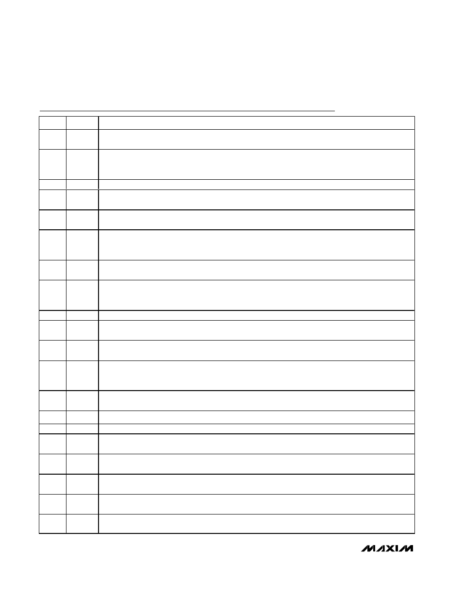
Pin Description
PIN
NAME
FUNCTION
1, 19
PGND
Power Ground. Sources of internal N-channel MOSFET power switches. Connect both PGND pins to GND as
close to the IC as possible.
2
DL1
External MOSFET Gate Drive Output for Auxiliary Controller 1. DL1 swings between POUT and GND with
typical 500mA drive current. Connect DL1 to the gate of the external switching N-channel MOSFET for
auxiliary controller 1.
3
ON1
Enable Input for Auxiliary Controller 1. Connect ON1 to POUT to automatically start auxiliary controller 1.
4
FB1
Feedback Input for Auxiliary Controller 1. Connect a feedback resistive voltage-divider from the output to FB1
to set the output voltage. Regulation voltage is V
REF
(1.25V).
5
COMP1
Compensation for Auxiliary Controller 1. Output of transconductance error amplifier. Connect a series resistor
and capacitor to GND to compensate the control loop. See Compensation Design.
6
DCON1
Maximum Duty-Cycle Control Input for Auxiliary Controller 1. Connect to POUT to set the default maximum
duty cycle. Connect a resistive voltage-divider from REF to DCON1 to set the maximum duty cycle between
40% and 90%. Pull DCON1 below 400mV to turn the controller off.
7, 22
POUT
Main Power Output. Source of P-channel MOSFET synchronous rectifier switch. Connect both POUT pins
together as close to the IC as possible.
8
DL2
External MOSFET Gate Drive Output for Auxiliary Controller 2. DL2 swings between POUT and GND with
typical 500mA drive current. Connect DL2 to the gate of the external switching N-channel MOSFET for
auxiliary controller 2.
9
ON2
Enable Input for Auxiliary Controller 2. Connect ON2 to POUT to automatically start auxiliary controller 2.
10
FB2
Feedback Input for Auxiliary Controller 2. Connect a feedback resistive voltage-divider from the output to FB2
to set the output voltage. Regulation voltage is V
REF
(1.25V).
11
COMP2
Compensation for Auxiliary Controller 2. Output of transconductance error amplifier. Connect a series resistor
and capacitor to GND to compensate the control loop. See Compensation Design.
12
DCON2
Maximum Duty-Cycle Control Input for Auxiliary Controller 2. Connect to POUT to set the default maximum
duty cycle. Connect a resistive voltage-divider from REF to DCON2 to set the maximum duty cycle between
40% and 90%. Pull DCON2 below 400mV to turn the controller off.
13
OUT
Internal Bias Supply Input. Connect to POUT through a resistor, and bypass OUT to GND with a capacitor.
See Compensation Design.
14
REF
1.250V Reference Output. Bypass REF to GND with a 0.1µF or greater ceramic capacitor.
15
GND
Analog Ground. Connect GND to PGND at a single point near the IC.
16
OSC
Oscillator Control. Connect a timing capacitor from OSC to GND and a timing resistor from OSC to POUT to
set the switching frequency between 100kHz and 1MHz. See Setting the Switching Frequency.
17
FBM
Main DC/DC Converter Feedback Input. Connect a feedback resistive voltage-divider from POUT to FBM to
set the output voltage. Regulation voltage is V
REF
(1.25V).
18
COMPM
Compensation for Main Controller. Output of transconductance error amplifier. Connect a series resistor and
capacitor to GND to compensate the control loop. See Compensation Design.
20,
21
LX
Main Power Switching Node. Drains of the internal P-channel and N-channel MOSFET switches. Connect the
LX pins together as close to the IC as possible.
23
RDYM
Main Converter Ready Output. An open-drain output sinks current when V
FBM
< 1.125V, indicating that the
main output is more than 10% out of regulation.