Max3625b, Table 4. crystal selection parameters, Crystal selection – Rainbow Electronics MAX3625В User Manual
Page 8: Crystal input layout, Interfacing with lvpecl outputs
MAX3625B
Crystal Selection
The crystal oscillator is designed to drive a fundamental
mode, AT-cut crystal resonator. See Table 4 for recom-
mended crystal specifications. See Figure 3 for external
capacitance connection.
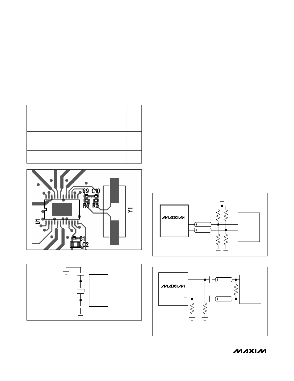
Crystal Input Layout
The crystal, trace, and two external capacitors should
be placed on the board as close as possible to the
MAX3625B’s X_IN and X_OUT pins to reduce crosstalk
of active signals into the oscillator. The example layout
shown in Figure 2 gives approximately 3pF of trace
plus footprint capacitance per side of the crystal. The
dielectric material is FR4 and dielectric thickness of the
reference board is 15 mils. Using a 25MHz crystal and
the capacitor values of C10 = 27pF and C9 = 33pF, the
measured output frequency accuracy is -14ppm at
+25°C ambient temperature.
Interfacing with LVPECL Outputs
The equivalent LVPECL output circuit is given in Figure 7.
These outputs are designed to drive a pair of 50
Ω trans-
mission lines terminated with 50
Ω to V
TT
= V
CC
- 2V. If a
separate termination voltage (V
TT
) is not available, other
termination methods can be used such as shown in
Figures 4 and 5. Unused outputs should be disabled and
may be left open. For more information on LVPECL termi-
nations and how to interface with other logic families, refer
to Application Note 291:
HFAN-01.0: Introduction to
LVDS, PECL, and CML
.
Low-Jitter, Precision Clock
Generator with Three Outputs
8
____________________________________________________
MAX3625B
Qx
82
Ω
Z
0
= 50
Ω
Qx
Z
0
= 50
Ω
82
Ω
130
Ω
130
Ω
+3.3V
HIGH
IMPEDANCE
Figure 4. Thevenin Equivalent of Standard PECL Termination
MAX3625B
Qx
150
Ω
100
Ω
Qx
Z
0
= 50
Ω
Z
0
= 50
Ω
HIGH
IMPEDANCE
150
Ω
0.1
μF
NOTE: AC-COUPLING IS OPTIONAL.
0.1
μF
Figure 5. AC-Coupled PECL Termination
Table 4. Crystal Selection Parameters
PARAMETER
SYMBOL
MIN
TYP
MAX
UNITS
Crystal Oscillation
Frequency
f
OSC
24.8 27 MHz
Shunt Capacitance
C
O
2.0
7.0
pF
Load Capacitance
C
L
18 pF
Equivalent Series
Resistance (ESR)
R
S
50
Maximum Crystal
Drive Level
300
μW
Figure 2. Crystal Layout
X_IN
X_OUT
27pF
CRYSTAL
(C
L
= 18pF)
33pF
Figure 3. Crystal, Capacitors Connection