Rainbow Electronics MAX3625В User Manual
Page 2
MAX3625B
Low-Jitter, Precision Clock
Generator with Three Outputs
2
_______________________________________________________________________________________
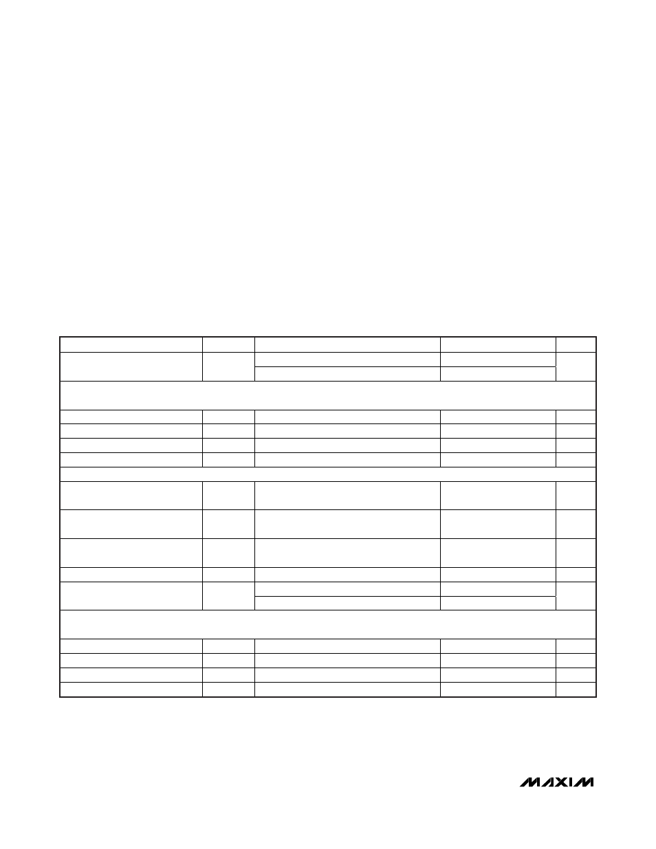
ABSOLUTE MAXIMUM RATINGS
ELECTRICAL CHARACTERISTICS
(V
CC
= +3.0V to +3.6V, T
A
= -40°C to +85°C, unless otherwise noted. Typical values are at V
CC
= +3.3V, T
A
= +25°C, unless other-
wise noted.) (Notes 1, 2)
Stresses beyond those listed under “Absolute Maximum Ratings” may cause permanent damage to the device. These are stress ratings only, and functional
operation of the device at these or any other conditions beyond those indicated in the operational sections of the specifications is not implied. Exposure to
absolute maximum rating conditions for extended periods may affect device reliability.
Supply Voltage Range V
CC
, V
CCA
,
V
CCO_A
, V
CCO_B
..............................................-0.3V to +4.0V
Voltage Range at REF_IN, IN_SEL,
FB_SEL, SELA[1:0], SELB[1:0],
QA_OE, QB_OE, MR, BYPASS ..............-0.3V to (V
CC
+ 0.3V)
Voltage Range at X_IN ..........................................-0.3V to +1.2V
Voltage Range at X_OUT ............................-0.3V to (V
CC
- 0.6V)
Current into QA, QA, QB0, QB0, QB1, QB1 .....................-56mA
Continuous Power Dissipation (T
A
= +70
°C)
24-Pin TSSOP (derate 26.7mW/
°C above +70°C) ..2133.3mW
Operating Junction Temperature Range ...........-55°C to +150°C
Storage Temperature Range .............................-65°C to +160°C
PARAMETER
SYMBOL
CONDITIONS
MIN
TYP
MAX
UNITS
IN_SEL = high
72
98
Power-Supply Current (Note 3)
I
CC
IN_SEL = low
74
mA
CONTROL INPUT CHARACTERISTICS
(SELA[1:0], SELB[1:0], FB_SEL, IN_SEL, QA_OE, QB_OE, MR,
BYPASS Pins)
Input Capacitance
C
IN
2
pF
Input Pulldown Resistor
R
PULLDOWN
Pins MR, FB_SEL
75
k
Input Logic Bias Resistor
R
BIAS
Pins SELA[1:0], SELB[1:0]
50
k
Input Pullup Resistor
R
PULLUP
Pins QA_OE, QB_OE, IN_SEL,
BYPASS
75
k
LVPECL OUTPUTS (QA,
QA, QB0, QB0, QB1, QB1 Pins)
Output High Voltage
V
OH
V
CC
-
1.18
V
CC
-
0.98
V
CC
-
0.83
V
Output Low Voltage
V
OL
V
CC
-
1.90
V
CC
-
1.7
V
CC
-
1.55
V
Peak-to-Peak Output-Voltage
Swing (Single-Ended)
(Note
2)
0.6
0.72
0.9
V
P-P
Clock Output Rise/Fall Time
20% to 80% (Note 2)
200
350
600
ps
PLL enabled
48
50
52
Output Duty-Cycle Distortion
PLL bypassed (Note 4)
45
50
55
%
LVCMOS/LVTTL INPUTS
(SELA[1:0], SELB[1:0], FB_SEL, IN_SEL, QA_OE, QB_OE, MR,
BYPASS Pins)
Input-Voltage High
V
IH
2.0
V
Input-Voltage Low
V
IL
0.8
V
Input High Current
I
IH
V
IN
= V
CC
80
μA
Input Low Current
I
IL
V
IN
= 0V
-80
μA