Applications information, Table 1. output frequency determination, Table 2. output divider configuration – Rainbow Electronics MAX3625В User Manual
Page 7: Table 3. pll divider configuration
MAX3625B
Low-Jitter, Precision Clock
Generator with Three Outputs
_______________________________________________________________________________________
7
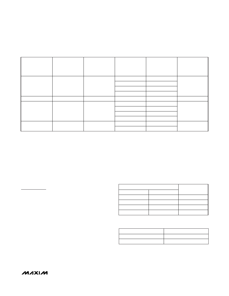
Table 1. Output Frequency Determination
CRYSTAL OR
CMOS INPUT
FREQUENCY
(MHz)
FEEDBACK
DIVIDER, M
VCO
FREQUENCY
(MHz)
OUTPUT
DIVIDER,
NA AND NB
OUTPUT
FREQUENCY
(MHz)
APPLICATIONS
2 312.5
4 156.25
5 125
25 25 625
10 62.5
Ethernet
25.78125 25 644.53125 4 161.132812
10Gbps
Ethernet
2 312.5
4 156.25
5 125
26.04166 24
625
10 62.5
Ethernet
2 318.75
26.5625 24 637.5
4 159.375
10G Fibre Channel
LVPECL Drivers
The high-frequency outputs—QA, QB0, and QB1—are
differential PECL buffers designed to drive transmission
lines terminated with 50
Ω to V
CC
- 2.0V. The maximum
operating frequency is specified up to 320MHz. The
outputs can be disabled, if not used. The outputs go to
a logic 0 when disabled.
Reset Logic/POR
During power-on, a power-on reset (POR) signal is gen-
erated to synchronize all dividers. An external master
reset (MR) signal is not required.
Applications Information
Power-Supply Filtering
The MAX3625B is a mixed analog/digital IC. The PLL
contains analog circuitry susceptible to random noise.
In addition to excellent on-chip power-supply noise
rejection, the MAX3625B provides a separate power-
supply pin, V
CCA
, for the VCO circuitry. Figure 1 illus-
trates the recommended power-supply filter network for
V
CCA
. The purpose of this design technique is to
ensure a clean power supply to the VCO circuitry and
to improve the overall immunity to power-supply noise.
This network requires that the power supply is +3.3V
±5%. Decoupling capacitors should be used on all
supply pins for best performance.
Output Divider Configuration
Table 2 shows the input settings required to set the out-
put dividers. Note that when the MAX3625B is in
bypass mode (BYPASS set low), the output dividers are
automatically set to divide by 1.
PLL Divider Configuration
Table 3 shows the input settings required to set the PLL
feedback divider.
Table 2. Output Divider Configuration
INPUT
SELA1/SELB1
SELA0/SELB0
NA/NB DIVIDER
0 0
ч10
0 1
ч2
1 0
ч4
1 1
ч5
Table 3. PLL Divider Configuration
FB_SEL INPUT
M DIVIDER
0
ч25
1
ч24