Detailed description, Pin description (continued) – Rainbow Electronics MAX3625В User Manual
Page 6
Detailed Description
The MAX3625B is a low-jitter clock generator designed
to operate at Ethernet and Fibre Channel frequencies. It
consists of an on-chip crystal oscillator, PLL, program-
mable dividers, and LVPECL output buffers. Using a
low-frequency clock (crystal or CMOS input) as a refer-
ence, the internal PLL generates a high-frequency out-
put clock with excellent jitter performance.
Crystal Oscillator
An integrated oscillator provides the low-frequency ref-
erence clock for the PLL. This oscillator requires an
external crystal connected between X_IN and X_OUT.
The crystal frequency is 24.8MHz to 27MHz.
REF_IN Buffer
An LVCMOS-compatible clock source can be connect-
ed to REF_IN to serve as the reference clock.
The LVCMOS REF_IN buffer is internally biased to the
threshold voltage (1.4V typ) to allow AC- or DC-cou-
pling, and is designed to operate up to 320MHz.
PLL
The PLL takes the signal from the crystal oscillator or
reference clock input and synthesizes a low-jitter, high-
frequency clock. The PLL contains a phase-frequency
detector (PFD), a lowpass filter, and a voltage-
controlled oscillator (VCO) with a 620MHz to 648MHz
operating range. The VCO is connected to the PFD
input through a feedback divider. See Table 3 for
divider values. The PFD compares the reference fre-
quency to the divided-down VCO output (f
VCO
/M) and
generates a control signal that keeps the VCO locked
to the reference clock. The high-frequency VCO output
clock is sent to the output dividers. To minimize noise-
induced jitter, the VCO supply (V
CCA
) is isolated from
the core logic and output buffer supplies.
Output Dividers
The output dividers are programmable to allow a range of
output frequencies. See Table 2 for the divider input set-
tings. The output dividers are automatically set to divide by
1 when the MAX3625B is in bypass mode (BYPASS = 0).
V
CC
V
CCA
10.5
Ω
+3.3V
±5%
0.01
μF
10
μF
0.01
μF
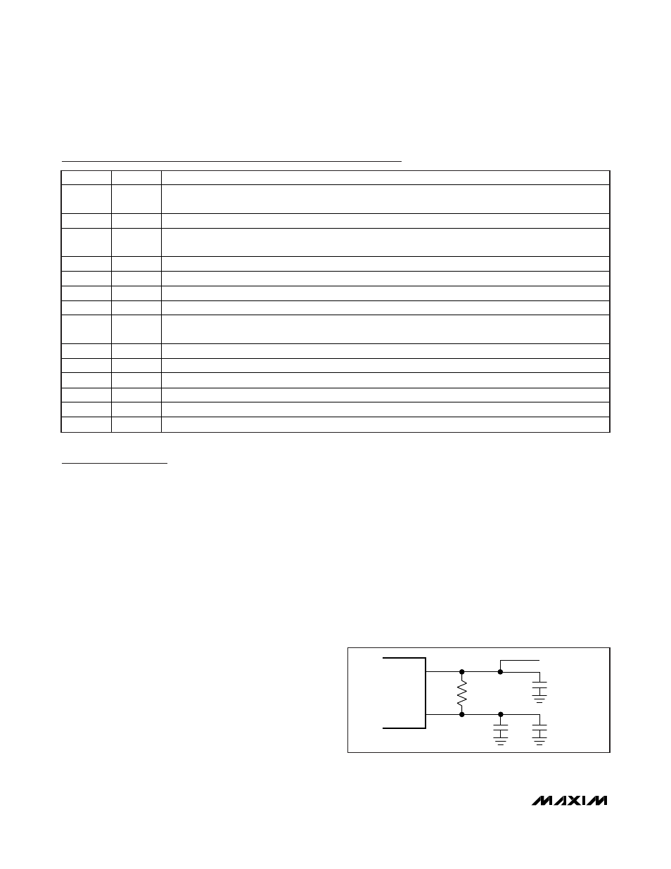
Figure 1. Analog Supply Filtering
MAX3625B
Low-Jitter, Precision Clock
Generator with Three Outputs
6
_______________________________________________________________________________________
Pin Description (continued)
PIN NAME
FUNCTION
10 V
CCA
Analog Power Supply for the VCO. Connect to +3.3V. For additional power-supply noise filtering, this
pin can connect to V
CC
through 10.5
as shown in Figure 1 (requires V
CC
= 3.3V ±5%).
11 V
CC
Core Power Supply. Connect to +3.3V.
12, 13
SELA0,
SELA1
LVCMOS/LVTTL Inputs. Control NA divider setting. See Table 2 for more information. 50k
input
impedance.
14 GND
Supply
Ground
15 X_OUT
Crystal
Oscillator
Output
16
X_IN
Crystal Oscillator Input
17
REF_IN
LVCMOS Reference Clock Input. Self-biased to allow AC- or DC-coupling.
18 IN_SEL
LVCMOS/LVTTL Input. Connect high or leave open to use a crystal. Connect low to use REF_IN. Has
internal 75k
pullup to V
CC
.
19
QB1
LVPECL, Inverting Clock Output
20
QB1
LVPECL, Noninverting Clock Output
21
QB0
LVPECL, Inverting Clock Output
22
QB0
LVPECL, Noninverting Clock Output
23 V
CCO_B
Power Supply for QB0 and QB1 Clock Output. Connect to +3.3V.
—
EP
Exposed Pad. Supply ground; connect to PCB ground for proper electrical and thermal performance.