Max3679a, 3v, low-jitter crystal to lvpecl clock generator, Interfacing with lvpecl outputs – Rainbow Electronics MAX3679A User Manual
Page 9: Interface models
MAX3679A
_______________________________________________________________________________________
9
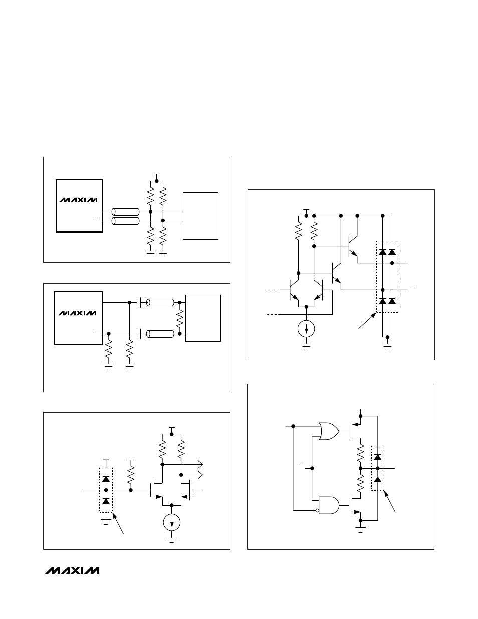
+3.3V, Low-Jitter Crystal to LVPECL
Clock Generator
Interfacing with LVPECL Outputs
The equivalent LVPECL output circuit is given in Figure 8.
These outputs are designed to drive a pair of 50
Ω trans-
mission lines terminated with 50
Ω to V
TT
= V
CC
- 2V. If a
separate termination voltage (V
TT
) is not available, other
termination methods can be used such as shown in
Figures 5 and 6. Unused outputs should be disabled and
can be left open. For more information on LVPECL termi-
nations and how to interface with other logic families,
refer to Application Note 291:
HFAN-01.0: Introduction to
LVDS, PECL, and CML
.
Interface Models
Figures 7, 8, and 9 show examples of interface models.
MAX3679A
Qx
82
Ω
Z
0
= 50
Ω
Qx
Z
0
= 50
Ω
82
Ω
130
Ω
130
Ω
+3.3V
HIGH
IMPEDANCE
Figure 5. Thevenin Equivalent of Standard PECL Termination
MAX3679A
Qx
150
Ω
100
Ω
Qx
Z
0
= 50
Ω
Z
0
= 50
Ω
HIGH
IMPEDANCE
150
Ω
0.1
μF
NOTE: AC-COUPLING IS OPTIONAL.
0.1
μF
Figure 6. AC-Coupled PECL Termination
14.5k
Ω
V
B
ESD
STRUCTURES
V
B
REF_IN
V
B
= 1.4V
V
CC
V
CC
Figure 7. Simplified REF_IN Pin Circuit Schematic
ESD
STRUCTURES
Qx
V
CC
Qx
Figure 8. Simplified LVPECL Output Circuit Schematic
10
Ω
10
Ω
ESD
STRUCTURES
QA_C
IN
DISABLE
V
DDO_A
Figure 9. Simplified LVCMOS Output Circuit Schematic