Pin configuration, Chip information, Layout considerations – Rainbow Electronics MAX3679A User Manual
Page 10: Exposed-pad package
MAX3679A
+3.3V, Low-Jitter Crystal to LVPECL
Clock Generator
10
______________________________________________________________________________________
MAX3679A
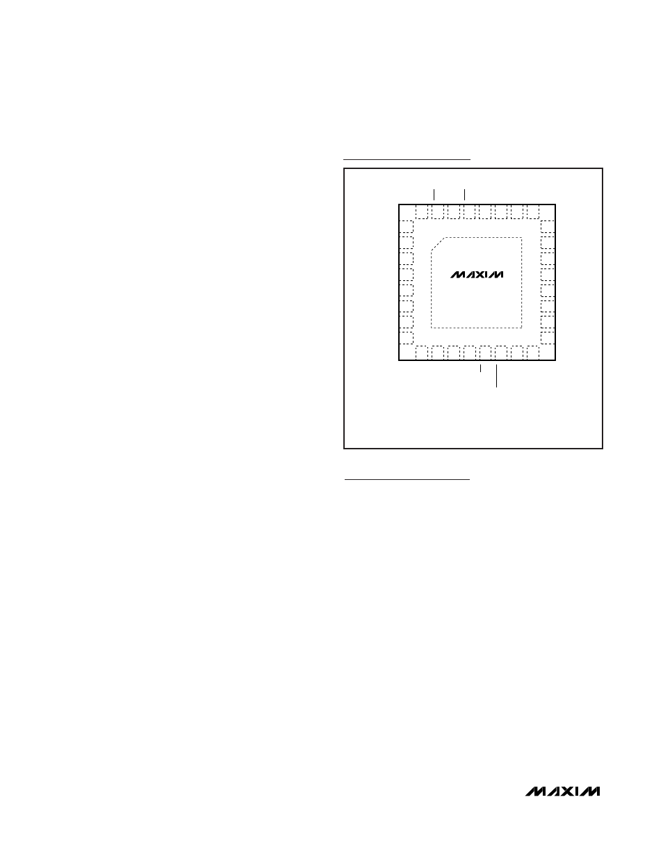
THIN QFN
(5mm
×
5mm)
TOP VIEW
5
6
4
3
20
19
21
V
DDO_A
QA
QA
BYPASS
RES1
22
QA_C
QB0
QB1
IN_SEL
QB0
REF_IN
X_IN
9
10
SELB1
12
13
14
15
31
32
30
28
27
26
SELB0
QAC_OE
SELA1
SELA0
QA_OE
GND
V
CCO_A
QB1
11
29
7
18
MR
V
CC
8
17
GNDO_A
V
CCA
QB0_OE
2
23
QB1_OE
GND
1
24
GND
RES0
X_OUT
16
25
V
CCO_B
+
*EP
*EXPOSED PAD CONNECTED TO GROUND.
Pin Configuration
Layout Considerations
The inputs and outputs are critical paths for the
MAX3679A, and care should be taken to minimize dis-
continuities on these transmission line. Here are some
suggestions for maximizing the MAX3679A’s perfor-
mance:
• An uninterrupted ground plane should be posi-
tioned beneath the clock I/Os.
• Ground pin vias should be placed close to the IC
and the input/output interfaces to allow a return
current path to the MAX3679A and the receive
devices.
• Supply decoupling capacitors should be placed
close to the MAX3679A supply pins.
• Maintain 100
Ω differential (or 50Ω single-ended)
transmission line impedance out of the MAX3679A.
• Use good high-frequency layout techniques and a
multilayer board with an uninterrupted ground
plane to minimize EMI and crosstalk.
Refer to the MAX3679A Evaluation Kit for more information.
Exposed-Pad Package
The exposed pad on the 32-pin TQFN package pro-
vides a very low inductance path for return current trav-
eling to the PCB ground plane. The pad is also
electrical ground on the MAX3679A and must be sol-
dered to the circuit board ground for proper electrical
performance.
Chip Information
TRANSISTOR COUNT: 10,780
PROCESS: BiCMOS