Max3679a, 3v, low-jitter crystal to lvpecl clock generator, Detailed description – Rainbow Electronics MAX3679A User Manual
Page 7: Applications information
MAX3679A
Detailed Description
The MAX3679A is a low-jitter clock generator designed
to operate at Ethernet frequencies. It consists of an on-
chip crystal oscillator, PLL, programmable dividers,
LVCMOS output buffer, and LVPECL output buffers.
Using a low-frequency clock (crystal or CMOS input) as
a reference, the internal PLL generates a high-frequen-
cy output clock with excellent jitter performance.
Crystal Oscillator
An integrated oscillator provides the low-frequency
reference clock for the PLL. This oscillator requires an
external crystal connected between X_IN and X_OUT.
Crystal frequency is 25MHz.
REF_IN Buffer
An LVCMOS-compatible clock source can be connected
to REF_IN to serve as the reference clock.
The LVCMOS REF_IN buffer is internally biased to allow
AC- or DC-coupling. It is designed to operate up to
320MHz.
PLL
The PLL takes the signal from the crystal oscillator or
reference clock input and synthesizes a low-jitter, high-
frequency clock. The PLL contains a phase-frequency
detector (PFD), a lowpass filter, and a 625MHz voltage-
controlled oscillator (VCO). The VCO output is connect-
ed to the PFD input through a feedback divider. The
PFD compares the reference frequency to the divided-
down VCO output (f
VCO
/25) and generates a control
signal that keeps the VCO locked to the reference
clock. The high-frequency VCO output clock is sent to
the output dividers. To minimize noise-induced jitter,
the VCO supply (V
CCA
) is isolated from the core logic
and output buffer supplies.
Output Dividers
The output divider is programmable to allow a range of
output frequencies. See Table 2 for the divider input
settings. The output dividers are automatically set to
divide by 1 when the MAX3679A is in bypass mode
(BYPASS = 0).
LVPECL Drivers
The high-frequency outputs—QA, QB0, and QB1—are
differential PECL buffers designed to drive transmission
lines terminated with 50
Ω to V
CC
- 2.0V. The maximum
operating frequency is specified up to 320MHz. Each
output can be individually disabled, if not used. The
outputs go to a logic 0 when disabled.
LVCMOS Driver
QA_C, the LVCMOS output, is designed to drive a sin-
gle-ended high-impedance load. The maximum operat-
ing frequency is specified up to 160MHz. This output
can be disabled by the QAC_OE pin if not used and
goes to a high impedance when disabled.
Reset Logic/POR
During power-on, the power-on reset (POR) signal is
generated to synchronize all dividers. An external mas-
ter reset (MR) signal is not required.
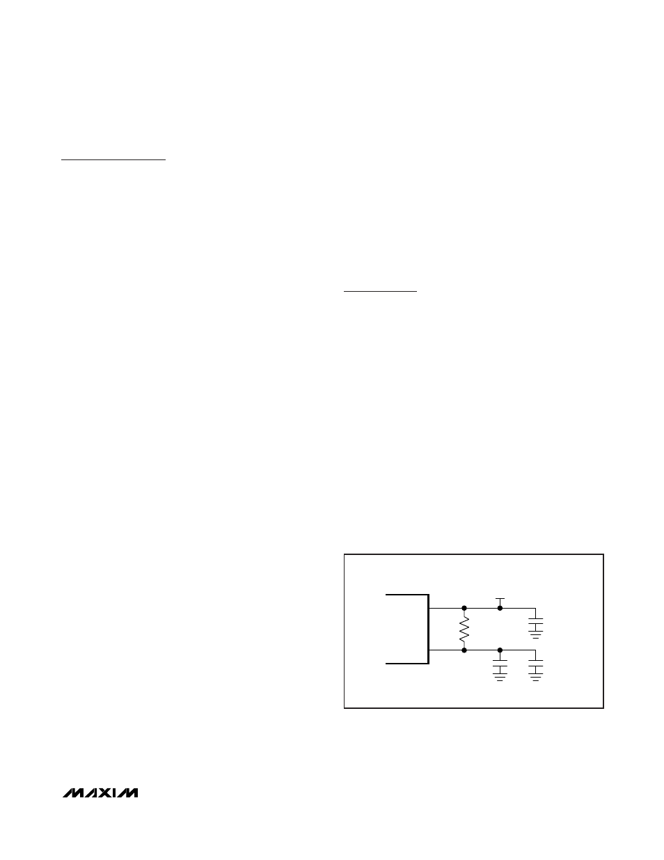
Applications Information
Power-Supply Filtering
The MAX3679A is a mixed analog/digital IC. The PLL
contains analog circuitry susceptible to random noise.
In addition to excellent on-chip power-supply noise
rejection, the MAX3679A provides a separate power-
supply pin, V
CCA
, for the VCO circuitry. Figure 2 illus-
trates the recommended power-supply filter network for
V
CCA
. The purpose of this design technique is to
ensure clean input power supply to the VCO circuitry
and to improve the overall immunity to power-supply
noise. This network requires that the power supply is
+3.3V ±5%. Decoupling capacitors should be used on
all other supply pins for best performance.
Output Divider Configuration
Table 2 shows the input settings required to set the out-
put dividers. Leakage in the OPEN case must be less
than 1µA. Note that when the MAX3679A is in bypass
mode (BYPASS set low), the output dividers are auto-
matically set to divide by 1.
V
CC
V
CCA
10.5
Ω
+3.3V
±5%
0.1
μF
10
μF
0.1
μF
Figure 2. Analog Supply Filtering
+3.3V, Low-Jitter Crystal to LVPECL
Clock Generator
_______________________________________________________________________________________
7