Table 2. output divider configuration, Table 3. crystal selection parameters, Table 1. output frequency determination – Rainbow Electronics MAX3679A User Manual
Page 8
MAX3679A
+3.3V, Low-Jitter Crystal to LVPECL
Clock Generator
8
_______________________________________________________________________________________
Crystal Selection
The crystal oscillator is designed to drive a fundamental
mode, AT-cut crystal resonator. See Table 3 for recom-
mended crystal specifications. See Figure 4 for external
capacitance connection.
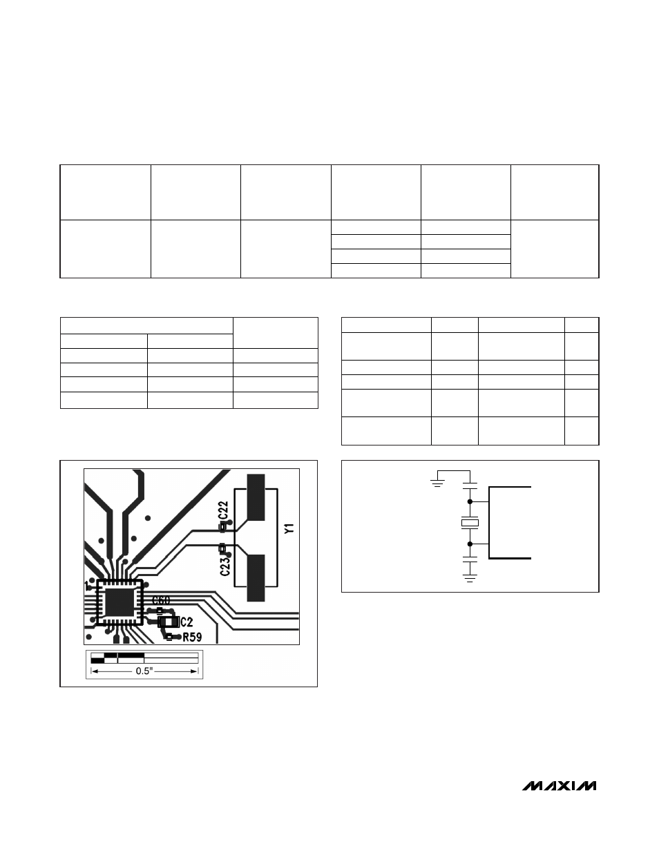
Crystal Input Layout and
Frequency Stability
The crystal, trace, and two external capacitors should
be placed on the board as close as possible to the
MAX3679A’s X_IN and X_OUT pins to reduce crosstalk
of active signals into the oscillator.
The layout shown in Figure 3 gives approximately 3pF
of trace plus footprint capacitors per side of the crystal
(Y1). The dielectric material is FR4 and dielectric thick-
ness of the reference board is 15 mils. Using a 25MHz
crystal and the capacitor values of C22 = 27pF and
C23 = 33pF, the measured output frequency accuracy
is -14ppm at +25°C ambient temperature.
Table 2. Output Divider Configuration
INPUT
SELA1/SELB1
SELA0/SELB0
NA/NB DIVIDER
0 0
ч2*
1 0 ч4
1 1 ч5
0 OPEN
÷10
Table 3. Crystal Selection Parameters
PARAMETER
SYMBOL
MIN
TYP
MAX
UNITS
Crystal Oscillation
Frequency
f
OSC
25 MHz
Shunt Capacitance
C
O
2.0
7.0
pF
Load Capacitance
C
L
18 pF
Equivalent Series
Resistance (ESR)
R
S
50
Maximum Crystal
Drive Level
300
μW
Table 1. Output Frequency Determination
XO OR CMOS
INPUT
FREQUENCY
(MHz)
FEEDBACK
DIVIDER, M
VCO
FREQUENCY
(MHz)
OUTPUT
DIVIDER,
NA AND NB
OUTPUT
FREQUENCY
(MHz)
APPLICATIONS
ч2 312.5
ч4 156.25
ч5 125
25 25 625
ч10 62.5
Ethernet
*Maximum guaranteed output frequency is 160MHz for CMOS
and 320MHz for LVPECL output.
Figure 3. Crystal Layout
X_IN
X_OUT
27pF
25MHz CRYSTAL
(C
L
= 18pF)
33pF
Figure 4. Crystal, Capacitors Connection