Timing diagram: read data transfer figure 5, Timing diagram: write data transfer figure 6 – Rainbow Electronics DS1202S User Manual
Page 8
DS1202, DS1202S
032697 8/11
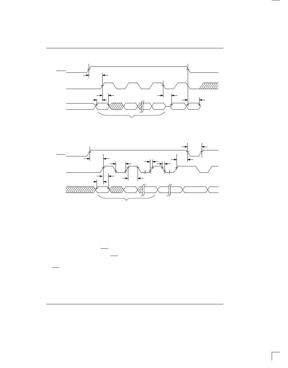
TIMING DIAGRAM: READ DATA TRANSFER Figure 5
t
CC
t
CDZ
t
CDD
t
CDH
t
DC
0
1
7
RESET
CLOCK
DATA INPUT/
OUTPUT
COMMAND BYTE
TIMING DIAGRAM: WRITE DATA TRANSFER Figure 6
t
CC
0
1
RESET
CLOCK
DATA INPUT/
OUTPUT
7
t
CWH
t
CCH
t
CDH
t
DC
t
F
t
R
t
CH
t
CL
COMMAND BYTE
NOTES:
1. All voltages are referenced to ground.
2. Logic one voltages are specified at a source current of 1 mA at V
CC
=5V and 0.4 mA at V
CC
=2V, V
OH
=V
CC
for
capacitive loads.
3. Logic zero voltages are specified at a sink current of 4 mA at V
CC
=5V and 1.5 mA at V
CC
=2V.
4. I
CC1
is specified with I/O open, RST set to a logic 0, and clock halt flag=0 (oscillator enabled).
5. I
CC
is specified with the I/O pin open, RST high, SCLK=2 MHz at V
CC
=5V; SCLK=500 KHz, V
CC
=2V and clock
halt flag=0 (oscillator enabled).
6. RST, SCLK, and I/O all have 40K
Ω
pull–down resistors to ground.
7. Measured at V
IH
=2.0V or V
IL
=0.8V and 10 ms maximum rise and fall time.
8. Measured at V
OH
=2.4V or V
OL
=0.4V.
9. Load capacitance = 50 pF.