Operation, Command byte, Address/command byte figure 2 – Rainbow Electronics DS1202S User Manual
Page 2
DS1202, DS1202S
032697 2/11
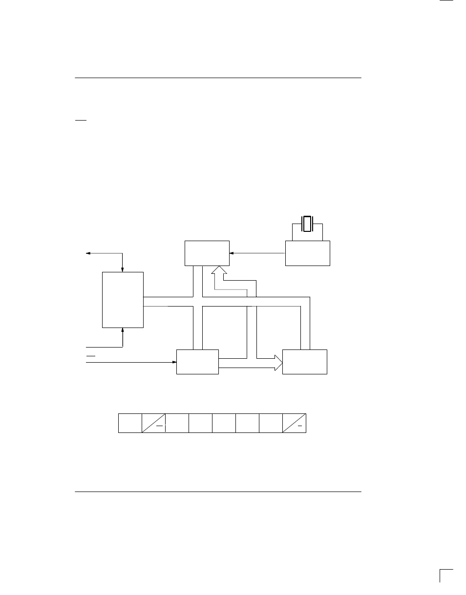
OPERATION
The main elements of the Serial Timekeeper are shown
in Figure 1: shift register, control logic, oscillator, real
time clock, and RAM. To initiate any transfer of data,
RST is taken high and eight bits are loaded into the shift
register providing both address and command informa-
tion. Data is serially input on the rising edge of the SCLK.
The first eight bits specify which of 32 bytes will be ac-
cessed, whether a read or write cycle will take place,
and whether a byte or burst mode transfer is to occur.
After the first eight clock cycles have occurred which
load the command word into the shift register, additional
clocks will output data for a read or input data for a write.
The number of clock pulses equals eight plus eight for
byte mode or eight plus up to 192 for burst mode.
COMMAND BYTE
The command byte is shown in Figure 2. Each data
transfer is initiated by a command byte. The MSB (Bit 7)
must be a logic 1. If it is zero, further action will be termi-
nated. Bit 6 specifies clock/calendar data if logic 0 or
RAM data if logic 1. Bits one through five specify the
designated registers to be input or output, and the LSB
(Bit 0) specifies a write operation (input) if logic 0 or read
operation (output) if logic 1. The command byte is al-
ways input starting with the LSB (bit 0).
DS1202 BLOCK DIAGRAM Figure 1
32.768 KHz
X2
X1
OSCILLATOR
AND DIVIDER
REAL TIME
CLOCK
DATA BUS
INPUT SHIFT
REGISTERS
COMMAND AND
CONTROL LOGIC
ADDRESS BUS
24 X 8 RAM
I/O
SCLK
RST
ADDRESS/COMMAND BYTE Figure 2
1
7
6
A4
5
A3
4
A2
3
A1
2
A0
1
RD
0
W
RAM
CK