Ds1870 ldmos rf power-amplifier bias controller, Ac electrical characteristics – Rainbow Electronics DS1870 User Manual
Page 5

DS1870
LDMOS RF Power-Amplifier Bias
Controller
_____________________________________________________________________
5
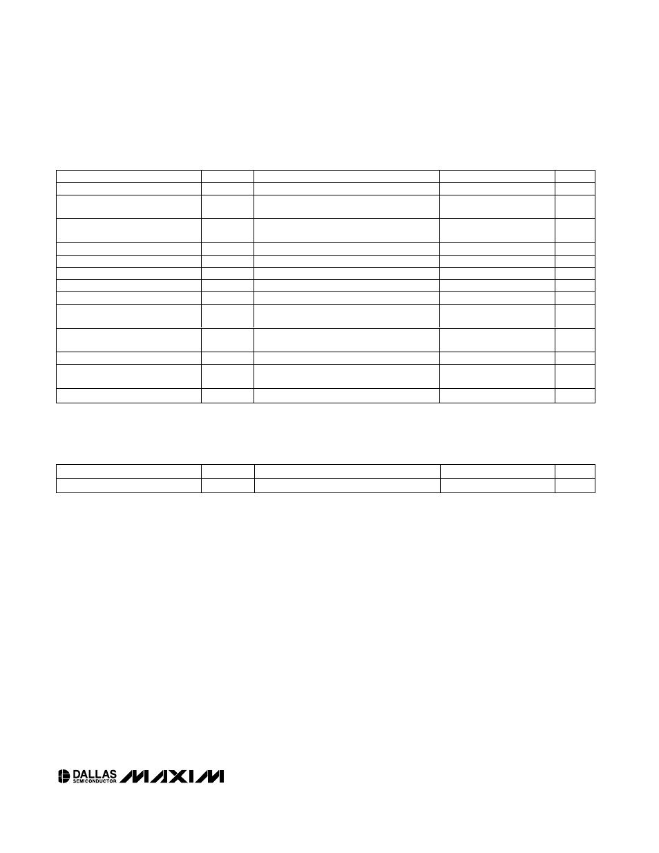
AC ELECTRICAL CHARACTERISTICS
(V
CC
= +4.5V to 5.5V, T
A
= -40°C to +95°C, timing referenced to V
IL(MAX)
and V
IH(MIN)
.) (Figure 3)
PARAMETER
SYMBOL
CONDITIONS
MIN
TYP
MAX
UNITS
SCL Clock Frequency
f
SCL
(Note 7)
0
400
kHz
Bus Free Time Between Stop and
Start Conditions
t
BUF
1.3
µs
Hold Time (Repeated) Start
Condition
t
HD:STA
0.6
µs
Low Period of SCL
t
LOW
1.3
µs
High Period of SCL
t
HIGH
0.6
µs
Data Hold Time
t
HD:DAT
0
0.9
µs
Data Setup Time
t
SU:DAT
100
ns
Start Setup Time
t
SU:STA
0.6
µs
SDA and SCL Rise Time
t
R
(Note 8)
20 +
0.1C
B
300
ns
SDA and SCL Fall Time
t
F
(Note 8)
20 +
0.1C
B
300
ns
Stop Setup Time
t
SU:STO
0.6
µs
SDA and SCL Capacitive
Loading
C
B
(Note 8)
400
pF
EEPROM Write Time
t
W
(Note 9)
10
20
ms
NONVOLATILE MEMORY CHARACTERISTICS
(V
CC
= +4.5V to 5.5V, T
A
= 0°C to +70°C.)
PARAMETER
SYMBOL
CONDITIONS
MIN
TYP
MAX
UNITS
Writes
+70°C (Note 5)
50,000
Note 1:
All voltages referenced to ground.
Note 2:
Supply current is measured with all logic inputs at their inactive state (SDA = SCL = V
CC
) and driven to well-defined logic
levels. All outputs are disconnected.
Note 3:
Absolute linearity is the difference of measured value from expected value at the DAC position. Expected value is a
straight line from measured minimum position to measured maximum position.
Note 4:
Relative linearity is the deviation of an LSB DAC setting change vs. the expected LSB change. Expected LSB change is
the slope of the straight line from measured minimum position to measured maximum position.
Note 5:
This parameter is guaranteed by design.
Note 6:
See Figure 1.
Note 7:
I
2
C interface timing shown is for fast-mode (400kHz) operation. This device is also backward compatible with I
2
C stan-
dard-mode timing.
Note 8:
C
B
—total capacitance of one bus line in picofarads.
Note 9:
EEPROM write begins after a stop condition occurs.
