Ds1870 ldmos rf power-amplifier bias controller – Rainbow Electronics DS1870 User Manual
Page 26

DS1870
LDMOS RF Power-Amplifier Bias
Controller
26
____________________________________________________________________
dition, and write the slave address byte (R/W = 0) and
the first memory address of the next memory row
before continuing to write data.
Acknowledge polling: Any time an EEPROM page is
written, the DS1870 requires the EEPROM write time
(t
W
) after the stop condition to write the contents of the
page to EEPROM. During the EEPROM write time, the
DS1870 will not acknowledge its slave address
because it is busy. It is possible to take advantage of
that phenomenon by repeatedly addressing the
DS1870, which allows the next page to be written as
soon as the DS1870 is ready to receive the data. The
alternative to acknowledge polling is to wait for maxi-
mum period of t
W
to elapse before attempting to write
again to the DS1870.
EEPROM write cycles: When EEPROM writes occur,
the DS1870 writes the whole EEPROM memory page,
even if only a single byte on the page was modified.
Writes that do not modify all 8 bytes on the page are
allowed and do not corrupt the remaining bytes of
memory on the same page. Because the whole page is
written, bytes on the page that were not modified dur-
ing the transaction are still subject to a write cycle. This
can result in a whole page being worn out over time by
writing a single byte repeatedly. Writing a page one
byte at a time wears the EEPROM out eight times faster
than writing the entire page at once. The DS1870’s
EEPROM write cycles are specified in the Nonvolatile
Memory Characteristics table. The specification shown
is at the worst-case temperature. It can handle approxi-
mately 10x that many writes at room temperature.
Writing to SRAM-shadowed EEPROM memory with SEE
= 1 does not count as an EEPROM write cycle when
evaluating the EEPROM’s estimated lifetime.
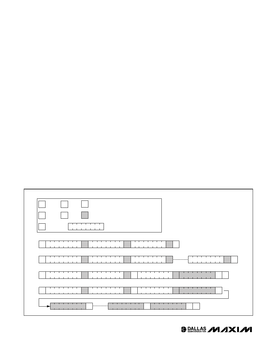
Reading a single byte from a slave: Unlike the write
operation that uses the memory address byte to define
where the data is to be written, the read operation occurs
at the present value of the memory address counter. To
read a single byte from the slave, the master generates a
start condition, writes the slave address byte with
R/W = 1, reads the data byte with a NACK to indicate the
end of the transfer, and generates a stop condition.
Manipulating the address counter for reads: A dummy
write cycle can be used to force the address counter to
a particular value. To do this, the master generates a
start condition, writes the slave address byte (R/W = 0),
writes the memory address where it desires to read, gen-
erates a repeated start condition, writes the slave
address byte (R/W = 1), reads data with ACK or NACK
as applicable, and generates a stop condition.
S
P
Sr
A
N
START
8 BITS ADDRESS OR DATA
REPEATED
START
STOP
ACK
NOT
ACK
WHITE BOXES INDICATE THE MASTER IS
CONTROLLING SDA
SHADED BOXES INDICATE THE SLAVE IS
CONTROLLING SDA
WRITE A SINGLE BYTE
WRITE UP TO AN 8-BYTE PAGE WITH A SINGLE TRANSACTION
READ A SINGLE BYTE WITH A DUMMY WRITE CYCLE TO MOVE THE ADDRESS COUNTER
READ MULTIPLE BYTES WITH A DUMMY WRITE CYCLE TO MOVE THE ADDRESS COUNTER
COMMUNICATIONS KEY
S
X
X
X
X
X
X
X
X
1
0
1
0
A
0
0
A
MEMORY ADDRESS
A
DATA
A
P
S
1
0
1
0
0
A
MEMORY ADDRESS
A
DATA
A
DATA
A
P
S
1
0
1
0
0
A
MEMORY ADDRESS
A
Sr
1 0
1
0
A
0
1
A
DATA
N
P
S
1
0
1
0
0
A
MEMORY ADDRESS
A
Sr
1 0
1
0
1
A
DATA
A
DATA
A
DATA
A
DATA
N
P
NOTES:
1) ALL BYTES ARE SENT MOST SIGNIFICANT BIT FIRST.
2) THE FIRST BYTE SENT AFTER A START
CONDITION IS ALWAYS THE SLAVE ADDRESS,
FOLLOWED BY THE READ/WRITE BIT.
A
1
A
2
A
0
A
1
A
2
A
0
A
1
A
2
A
0
A
1
A
2
A
1
A
2
A
0
A
1
A
2
Figure 5. I
2
C Communications Examples
