Ds1870 ldmos rf power-amplifier bias controller, Table 6. lut addresses for vd or idx values – Rainbow Electronics DS1870 User Manual
Page 12

DS1870
LDMOS RF Power-Amplifier Bias
Controller
12
____________________________________________________________________
The temperature tables (LUT 2 and LUT 3) are 72 bytes
each. This allows the biasing to be adjusted every 2°C
between -40°C and +102°C. Temperatures less than
-40°C or greater than 102°C use the -40°C or 102°C
values, respectively. The values in the temperature
tables are 8-bit unsigned values (0 to 255 decimal) that
allow the potentiometer to be set to any position as a
function of the temperature. The temperature LUTs
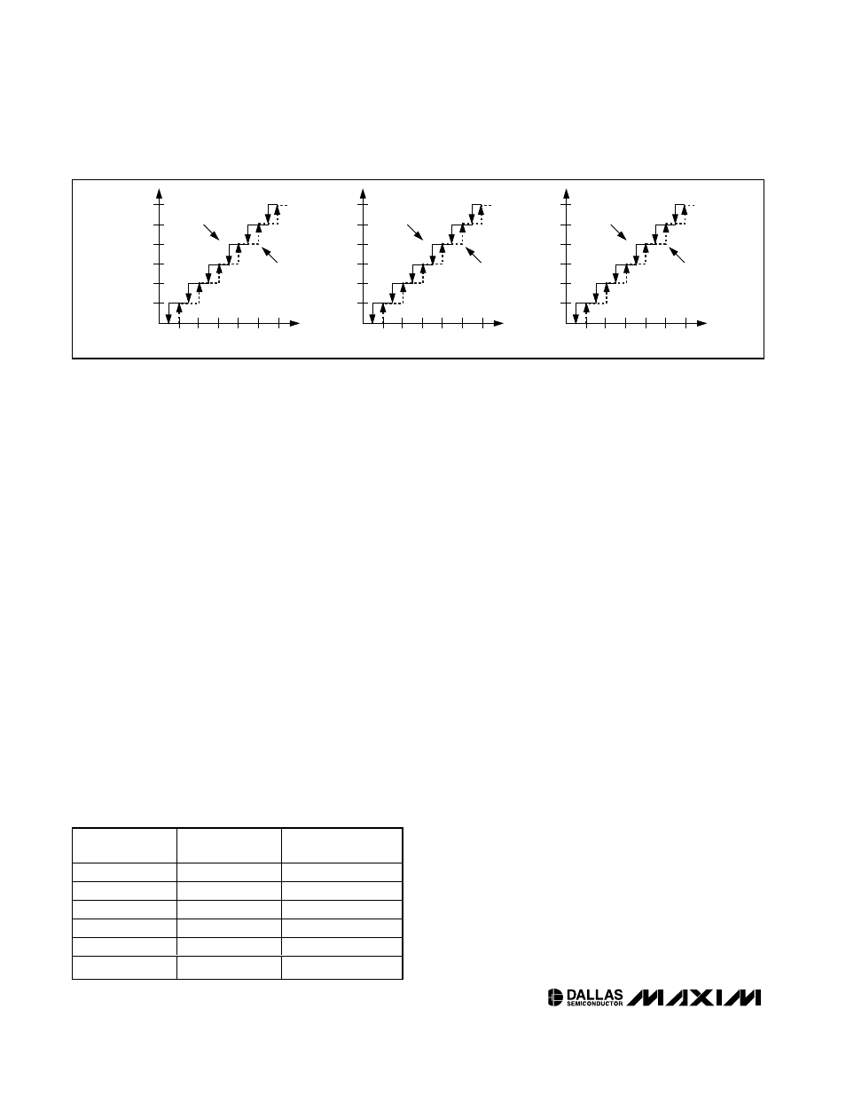
have 1°C hysteresis (Figure 1) to prevent the poten-
tiometer’s position from chattering in the event the tem-
perature remains near a LUT switching point. Table 5
shows how the DS1870 determines the temperature
tables index as a function of temperature.
The drain tables (LUT 4 and LUT5) are 64 bytes each,
and they can be indexed either by the drain voltage or
the drain current corresponding to the potentiometer.
The VD1 control bit determines if the voltage sensed on
V
D
or I
D1
adjusts the POT1 Drain LUT, and the VD2
control bit determines if the voltage sensed on V
D
or
I
D2
controls the POT2 Drain LUT. The VD1 and VD2
control bits are located in register 85h of memory table
1. The drain tables are programmed with an 8-bit
signed value (-128 to +127 decimal) that allow a rela-
tive offset from the temperature LUT values determined
by the amplifier’s drain characteristics.
The drain LUTs are indexed either by the upper half of
the V
D
range or the lower half of its corresponding I
DX
range. Table 6 shows how the index is determined
based on the V
D
or I
DX
values. Hysteresis equal to
0100h is also implemented on the drain monitor
(Figure 1) to ensure that voltages close to a switching
point do not cause the potentiometer position to chatter
between two LUT values. The drain LUT index values are
specified in hexadecimal because the hexadecimal val-
ues are applicable regardless of the gain and offset cali-
bration of the DS1870.
Manual Mode
During normal operation, the potentiometer position is
automatically modified once per conversion cycle
based on the ADC results. The DS1870 can either stop
the update function all together by using the B/O_en
bit, or the temperature and drain LUT indexes can be
manually controlled by using the Index_en bit. These
bits are located in the Man DAC register located in
memory table 1, byte AFh. More information about
these bits is in the Register Description section.
Voltage-Monitor Calibration
The DS1870 can scale each analog voltage’s gain and
offset to produce the desired digital result. Each of the
inputs (V
CC
V
D
, I
D1
, I
D2
) has a unique register for the
gain and offset (in memory table 1) allowing them to be
individually calibrated. Additionally, the DS1870 offers
the ability to provide a temperature offset to allow the
temperature measurement to be compensated to
account for the difference in temperature between the
DS1870 and the device it is biasing.
To scale the gain and offset of the converter for a spe-
cific input, you must first know the relationship between
the analog input and the expected digital result. The
input that would produce a digital result of all zeros is
the null value (normally this input is GND). The input
that would produce a digital result of all ones (FFF8h) is
LUT ADDRESS
(hex)
V
D
VALUE
(hex)
I
DX
VALUE
(hex)
80
≤ 8000
0000
81
8200
0200
82
8400
0400
…
…
…
BE
FC00
7C00
BF
≥ FE00
≥ 7E00
Table 6. LUT Addresses for VD or IDX
Values
9Ah
99h
98h
97h
96h
95h
2
4
6
8
10
12
TEMPERATURE (°C)
MEMOR
Y LOCA
TION
MEMOR
Y LOCA
TION
MEMOR
Y LOCA
TION
9Ah
99h
98h
97h
96h
95h
AA00 AC00 AEOO B000 B200 B400
DRAIN VOLTAGE CONVERSION (HEX)
9Ah
99h
98h
97h
96h
95h
2A00 2C00 2E00 3000 3200 3400
DRAIN CURRENT CONVERSION (HEX)
INCREASING
TEMPERATURE
INCREASING
DRAIN VOLTAGE
INCREASING
DRAIN CURRENT
DECREASING
TEMPERATURE
DECREASING
DRAIN VOLTAGE
DECREASING
DRAIN CURRENT
Figure 1. LUT Hysteresis
