Operation, Figure 4. block diagram clock accuracy, Address map – Rainbow Electronics DS1672 User Manual
Page 7: Table 1. registers
DS1672
7 of 12
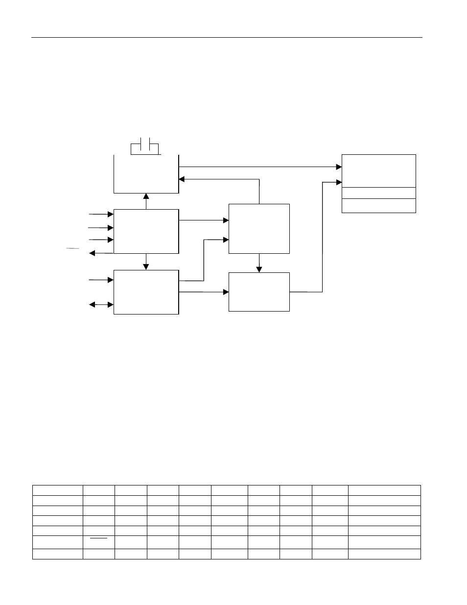
OPERATION
The block diagram in Figure 4 shows the main elements of the DS1672. As shown, communications to
and from the DS1672 occur serially over a 2-wire, bidirectional bus. The DS1672 operates as a slave
device on the serial bus. Access is obtained by implementing a START condition and providing a device
identification code followed by a register address. Subsequent registers can be accessed sequentially until
a STOP condition is executed.
Figure 4. Block Diagram
Clock Accuracy
The accuracy of the clock is dependent upon the accuracy of the crystal and the accuracy of the match
between the capacitive load of the oscillator circuit and the capacitive load for which the crystal was
trimmed. Additional error will be added by crystal frequency drift caused by temperature shifts. External
circuit noise coupled into the oscillator circuit may result in the clock running fast. Refer to Application
Note 5: “Crystal Considerations with Dallas Real-Time Clocks” for detailed information.
Address Map
The counter is accessed by reading or writing the first 4 bytes of the DS1672 (00h–03h). The control
register and trickle charger are accessed by reading or writing the appropriate register bytes as illustrated
in Table 1. If the master continues to send or request more data after the address pointer has reached 05h,
the address pointer will wrap around to location 00h.
Table 1. Registers
ADDRESS
B7
B6
B5
B4
B3
B2
B1
B0
FUNCTION
00h
LSB
Counter Byte 1
01h
Counter Byte 2
02h
Counter Byte 3
03h
MSB
Counter Byte 4
04h
EOSC
Control
05h
TCS
TCS
TCS
TCS
DS
DS
RS
RS
Trickle Charger
32-BIT
COUNTER
(4 BYTES)
SERIAL BUS
INTERFACE
OSCILLATOR
AND DIVIDER
POWER
CONTROL
ADDRESS
REGISTER
CONTROL
LOGIC
V
CC
V
BACKUP
GND
SCL
SDA
CONTROL
TRICKLE CHARGER
X1
X2
RST