Address map, Table 2. address map – Rainbow Electronics DS1393 User Manual
Page 13
Address Map
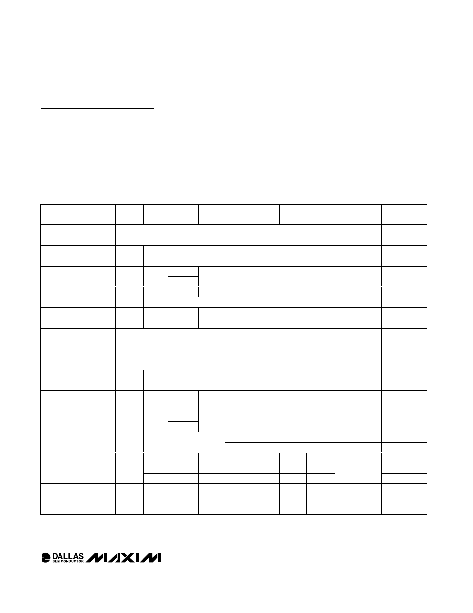
Table 2 shows the address map for the DS1390–
DS1393 RTC and RAM registers. The RTC registers are
located in address locations 00h to 0Fh in read mode,
and 80h to 8Fh in write mode. During a multibyte
access, when the address pointer reaches 0Fh, it
wraps around to location 00h. On the falling edge of the
CS pin (DS1390/DS1391) or the rising edge of CE
(DS1392/DS1393), the current time is transferred to a
second set of registers. The time information is read
from these secondary registers, while the clock may
continue to run. This eliminates the need to re-read the
registers if the main registers update during a read. To
avoid rollover issues when writing to the time and date
registers, all registers should be written before the hun-
dredths-of-seconds registers reaches 99 (BCD).
DS1390/DS1391/DS1392/DS1393
Low-Voltage SPI/3-Wire RTCs with
Trickle Charger
____________________________________________________________________
13
WRITE
ADDRESS
READ
ADDRESS
BIT 7
BIT 6
BIT 5
BIT 4
BIT 3
BIT 2
BIT 1
BIT 0
FUNCTION
RANGE
80h
00h
Tenths of Seconds
Hundredths of Seconds
Hundredths
of Seconds
0–99 BCD
81h
01h
0
10 Seconds
Seconds
Seconds
00–59 BCD
82h
02h
0
10 Minutes
Minutes
Minutes
00–59 BCD
AM/PM
83h
03h
0
12/24
10 Hour
10
Hour
Hour
Hours
1–12 +AM/PM
00–23 BCD
84h
04h
0
0
0
0
0
Day
Day
1–7 BCD
85h
05h
0
0
10 Date
Date
Date
01–31 BCD
86h
06h
Century
0
0
10
Month
Month
Month/
Century
01–12 +
Century BCD
87h
07h
10 Year
Year
Year
00–99 BCD
88h
08h
Tenths of Seconds
Hundredths of Seconds
Alarm
Hundredths
of Seconds
0–99 BCD
89h
09h
AM1
10 Seconds
Seconds
Alarm
00–59 BCD
8Ah
0Ah
AM2
10 Minutes
Minutes
Alarm
00–59 BCD
AM/PM
8Bh
0Bh
AM3
12/24
10 Hour
10
Hour
Hour
Alarm Hours
1–12 +
AM/PM
00–23 BCD
Day
Alarm Day
1–7 BCD
8Ch
0Ch
AM4
DY/DT
10 Date
Date
Alarm Date
1–31 BCD
0
BBSQI
RS2
RS1
INTCN
0
AIE
DS1390/93
0
X
X
X
X
0
X
DS1391
8Dh
0Dh
EOSC
0
BBSQI
RS2
RS1
ESQW
0
AIE
Control
DS1392
8Eh
0Eh
OSF
0
0
0
0
0
0
AF
Status
—
8Fh
0Fh
TCS3
TCS2
TCS1
TCS0
DS1
DS0
ROUT1
ROUT0
Trickle
Charger
—
Table 2. Address Map
Note: Unless otherwise specified, the state of the registers is not defined when power (V
CC
and V
BACKUP
) is first applied.
X = General-purpose read/write bit.
0 = Always reads as zero.