Avr cpu core, Introduction, Architectural overview – Rainbow Electronics ATmega32L User Manual
Page 6: Atmega32(l)
6
ATmega32(L)
2503C–AVR–10/02
AVR CPU Core
Introduction
This section discusses the AVR core architecture in general. The main function of the
CPU core is to ensure correct program execution. The CPU must therefore be able to
access memories, perform calculations, control peripherals, and handle interrupts.
Architectural Overview
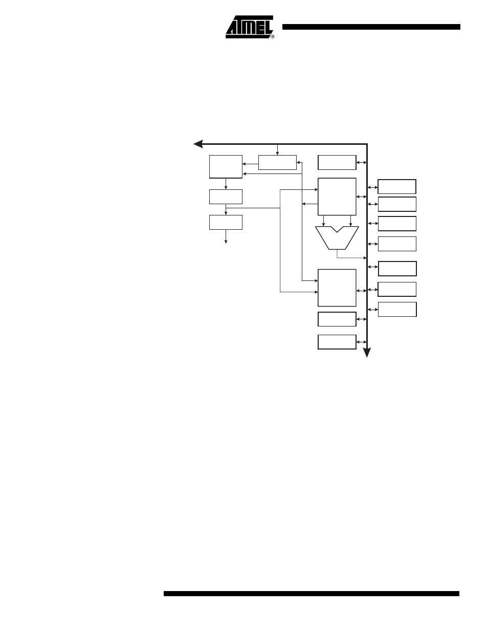
Figure 3. Block Diagram of the AVR MCU Architecture
In order to maximize performance and parallelism, the AVR uses a Harvard architecture
– with separate memories and buses for program and data. Instructions in the program
memory are executed with a single level pipelining. While one instruction is being exe-
cuted, the next instruction is pre-fetched from the program memory. This concept
enables instructions to be executed in every clock cycle. The program memory is In-
System Reprogrammable Flash memory.
The fast-access Register file contains 32 x 8-bit general purpose working registers with
a single clock cycle access time. This allows single-cycle Arithmetic Logic Unit (ALU)
operation. In a typical ALU operation, two operands are output from the Register file, the
operation is executed, and the result is stored back in the Register file – in one clock
cycle.
Six of the 32 registers can be used as three 16-bit indirect address register pointers for
Data Space addressing – enabling efficient address calculations. One of the these
address pointers can also be used as an address pointer for look up tables in Flash Pro-
gram memory. These added function registers are the 16-bit X-, Y-, and Z-register,
described later in this section.
The ALU supports arithmetic and logic operations between registers or between a con-
stant and a register. Single register operations can also be executed in the ALU. After
Flash
Program
Memory
Instruction
Register
Instruction
Decoder
Program
Counter
Control Lines
32 x 8
General
Purpose
Registrers
ALU
Status
and Control
I/O Lines
EEPROM
Data Bus 8-bit
Data
SRAM
Direct Addressing
Indirect Addressing
Interrupt
Unit
SPI
Unit
Watchdog
Timer
Analog
Comparator
I/O Module 2
I/O Module1
I/O Module n