Atmega32(l) – Rainbow Electronics ATmega32L User Manual
Page 234
234
ATmega32(L)
2503C–AVR–10/02
Note:
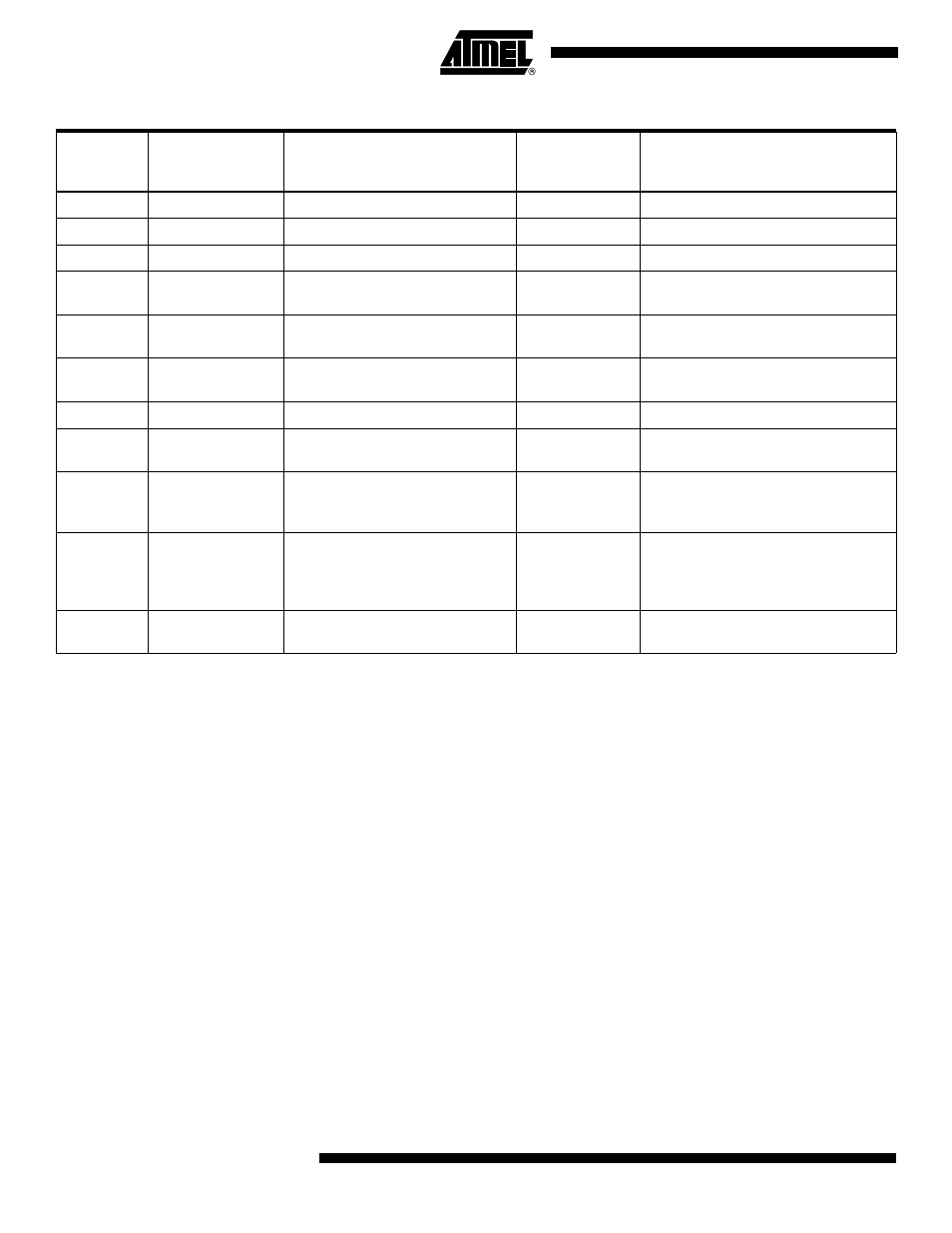
Incorrect setting of the switches in Figure 123 will make signal contention and may damage the part. There are several input
choices to the S&H circuitry on the negative input of the output comparator in Figure 123. Make sure only one path is selected
from either one ADC pin, Bandgap reference source, or Ground.
MUXEN_2
Input
Input Mux bit 2
0
0
MUXEN_1
Input
Input Mux bit 1
0
0
MUXEN_0
Input
Input Mux bit 0
1
1
NEGSEL_2
Input
Input Mux for negative input for
differential signal, bit 2
0
0
NEGSEL_1
Input
Input Mux for negative input for
differential signal, bit 1
0
0
NEGSEL_0
Input
Input Mux for negative input for
differential signal, bit 0
0
0
PASSEN
Input
Enable pass-gate of gain stages.
1
1
PRECH
Input
Precharge output latch of
comparator. (Active low)
1
1
SCTEST
Input
Switch-cap TEST enable. Output
from x10 gain stage send out to
Port Pin having ADC_4
0
0
ST
Input
Output of gain stages will settle
faster if this signal is high first two
ACLK periods after AMPEN goes
high.
0
0
VCCREN
Input
Selects Vcc as the ACC reference
voltage.
0
0
Table 92. Boundary-scan Signals for the ADC (Continued)
Signal
Name
Direction as Seen
from the ADC
Description
Recommended
Input when Not
in Use
Output Values when Recommended
Inputs are used, and CPU is not
Using the ADC