Scanning the reset pin, Scanning the clock pins, Atmega32(l) – Rainbow Electronics ATmega32L User Manual
Page 229
229
ATmega32(L)
2503C–AVR–10/02
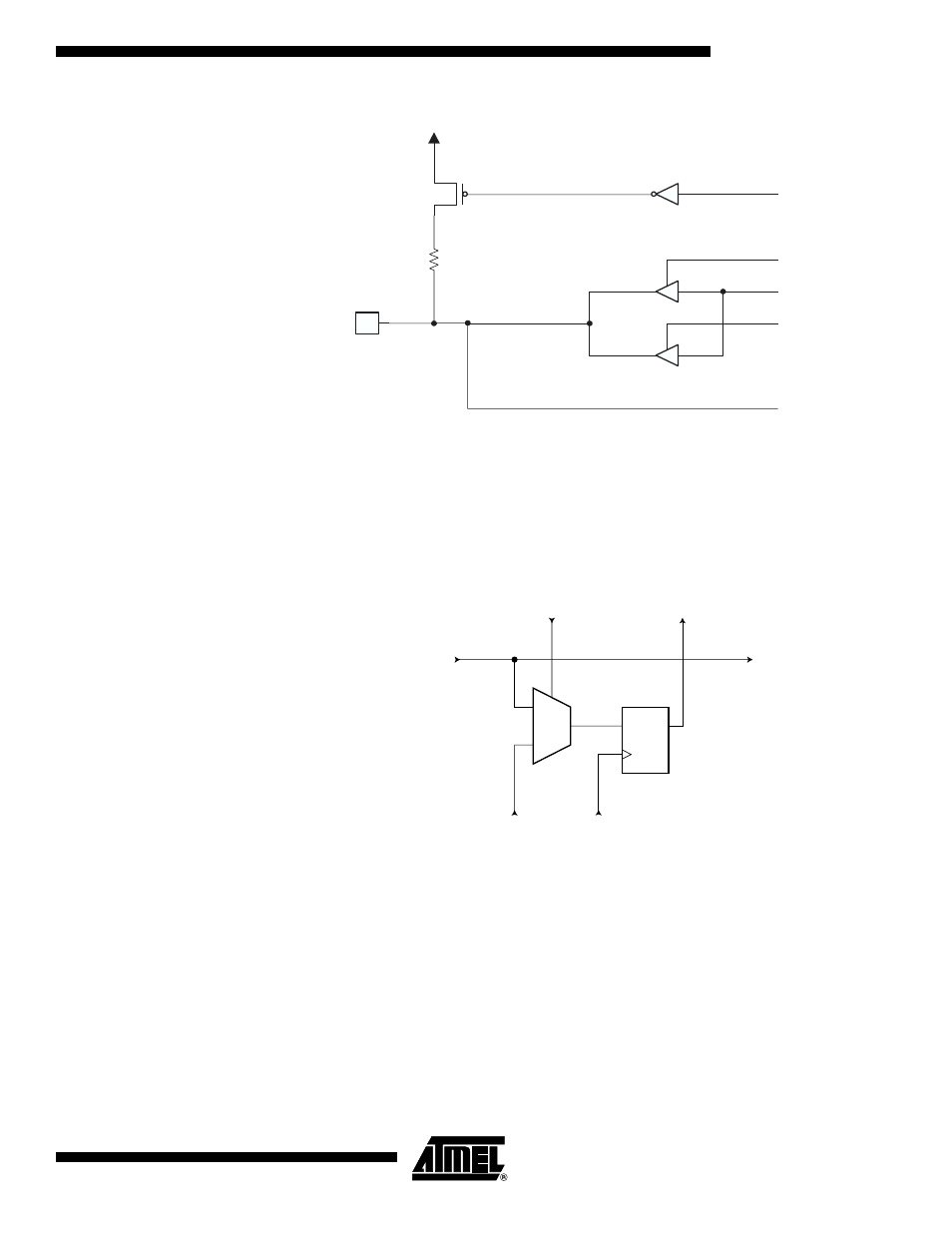
Figure 118. Additional Scan Signal for the Two-wire Interface
Scanning the RESET Pin
The RESET pin accepts 5V active low logic for standard reset operation, and 12V active
high logic for High Voltage Parallel Programming. An observe-only cell as shown in Fig-
ure 119 is inserted both for the 5V reset signal; RSTT, and the 12V reset signal;
RSTHV.
Figure 119. Observe-only Cell
Scanning the Clock Pins
The AVR devices have many clock options selectable by fuses. These are: Internal RC
Oscillator, External RC, External Clock, (High Frequency) Crystal Oscillator, Low Fre-
quency Crystal Oscillator, and Ceramic Resonator.
Figure 120 shows how each Oscillator with external connection is supported in the scan
chain. The Enable signal is supported with a general boundary-scan cell, while the
Oscillator/Clock output is attached to an observe-only cell. In addition to the main clock,
the Timer Oscillator is scanned in the same way. The output from the internal RC Oscil-
lator is not scanned, as this Oscillator does not have external connections.
Pxn
PUExn
ODxn
IDxn
TWIEN
OCxn
Slew-rate Limited
SRC
0
1
D
Q
From
Previous
Cell
ClockDR
ShiftDR
To
Next
Cell
From System Pin
To System Logic
FF1