Alternate functions of port c, Atmega32(l) – Rainbow Electronics ATmega32L User Manual
Page 58
58
ATmega32(L)
2503C–AVR–10/02
Alternate Functions of Port C
The Port C pins with alternate functions are shown in Table 28. If the JTAG interface is
enabled, the pull-up resistors on pins PC5(TDI), PC3(TMS) and PC2(TCK) will be acti-
vated even if a reset occurs.
The alternate pin configuration is as follows:
• TOSC2 – Port C, Bit 7
TOSC2, Timer Oscillator pin 2: When the AS2 bit in ASSR is set (one) to enable asyn-
chronous clocking of Timer/Counter2, pin PC7 is disconnected from the port, and
becomes the inverting output of the Oscillator amplifier. In this mode, a Crystal Oscillator
is connected to this pin, and the pin can not be used as an I/O pin.
• TOSC1 – Port C, Bit 6
TOSC1, Timer Oscillator pin 1: When the AS2 bit in ASSR is set (one) to enable asyn-
chronous clocking of Timer/Counter2, pin PC6 is disconnected from the port, and
becomes the input of the inverting Oscillator amplifier. In this mode, a Crystal Oscillator
is connected to this pin, and the pin can not be used as an I/O pin.
• TDI – Port C, Bit 5
TDI, JTAG Test Data In: Serial input data to be shifted in to the Instruction Register or
Data Register (scan chains). When the JTAG interface is enabled, this pin can not be
used as an I/O pin.
• TDO – Port C, Bit 4
TDO, JTAG Test Data Out: Serial output data from Instruction register or Data Register.
When the JTAG interface is enabled, this pin can not be used as an I/O pin.
The TD0 pin is tri-stated unless TAP states that shifts out data are entered.
• TMS – Port C, Bit 3
TMS, JTAG Test Mode Select: This pin is used for navigating through the TAP-controller
state machine. When the JTAG interface is enabled, this pin can not be used as an I/O
pin.
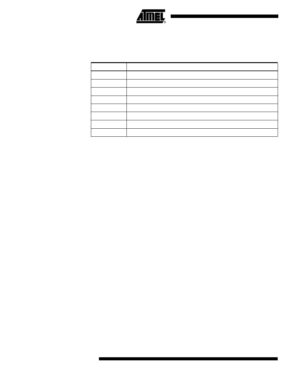
Table 28. Port C Pins Alternate Functions
Port Pin
Alternate Function
PC7
TOSC2 (Timer Oscillator Pin 2)
PC6
TOSC1 (Timer Oscillator Pin 1)
PC5
TDI (JTAG Test Data In)
PC4
TDO (JTAG Test Data Out)
PC3
TMS (JTAG Test Mode Select)
PC2
TCK (JTAG Test Clock)
PC1
SDA (Two-wire Serial Bus Data Input/Output Line)
PC0
SCL (Two-wire Serial Bus Clock Line)