Rainbow Electronics AT84AD001B User Manual
Page 10

10
AT84AD001B
2153C–BDC–04/04
Note:
One analog input on both cores, clock I samples the analog input on the rising and falling edges. The calibration
phase is necessary. The gain setting is 0 dB, one input clock I, no standby mode, 1:1 DMUX, FiSDA adjustment.
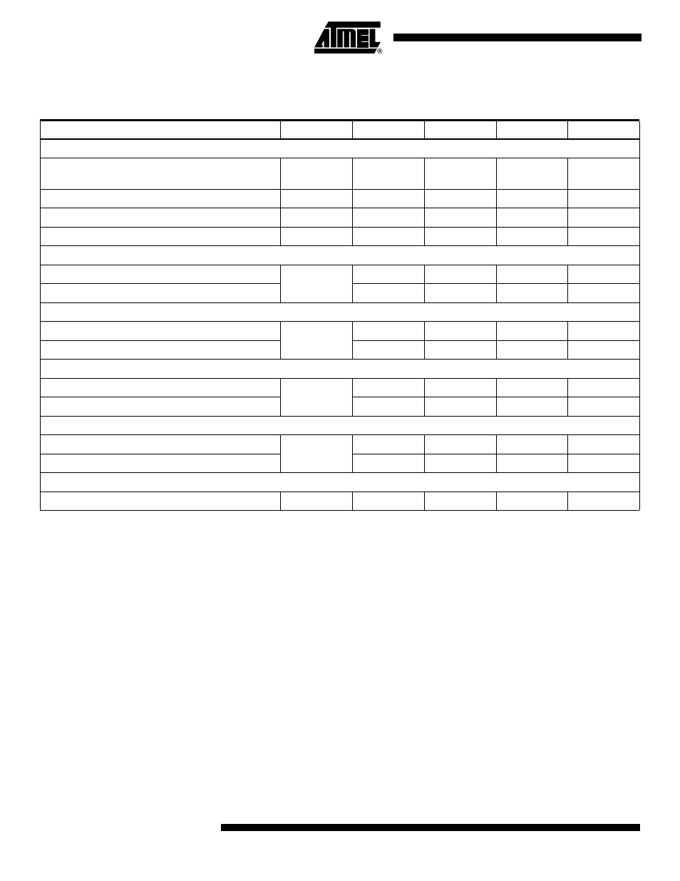
Table 6. AC Performances in Interlace Mode
Parameter
Symbol
Min
Typ
Max
Unit
Interlace Mode
Maximum equivalent clock frequency Fint = 2 x Fs
Where Fs = external clock frequency
F
int
2
Gsps
Minimum clock frequency
F
int
20
Msps
Differential non-linearity in interlace mode
intDNL
0.25
LSB
Integral non-linearity in interlace mode
intINL
0.5
LSB
Signal-to-noise Ratio in Interlace Mode
Fint = 2 Gsps
Fin = 20 MHz
iSNR
42
dBc
Fint = 2 Gsps
Fin = 250 MHz
40
dBc
Effective Number of Bits in Interlace Mode
Fint = 2 Gsps
Fin = 20 MHz
iENOB
7.1
Bits
Fint = 2 Gsps
Fin = 250 MHz
6.8
Bits
Total Harmonic Distortion in Interlace Mode
Fint = 2 Gsps
Fin = 20 MHz
|iTHD|
52
dBc
Fint = 2 Gsps
Fin = 250 MHz
49
dBc
Spurious Free Dynamic Range in Interlace Mode
Fint = 2 Gsps
Fin = 20 MHz
|iSFDR|
54
dBc
Fint = 2 Gsps
Fin = 250 MHz
52
dBc
Two-tone Inter-modulation Distortion (Single Channel) in Interlace Mode
F
IN1
= 249 MHz , F
IN2
= 251 MHz at F
int
= 2 Gsps
iIMD
-54
dBc
