Preload of registered outputs, Power-up reset, Pin capacitance – Rainbow Electronics ATF750CL User Manual
Page 10: Atf750c(l)
ATF750C(L)
10
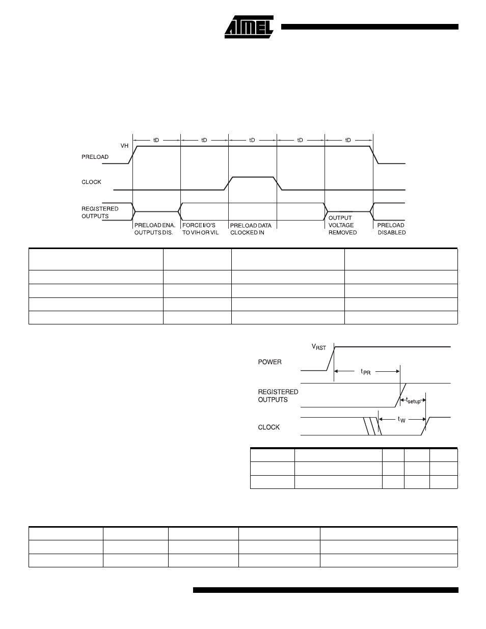
Preload of Registered Outputs
The ATF750C(L)’s registers are provided with circuitry to
allow loading of each register asynchronously with either a
high or a low. This feature will simplify testing since any
state can be forced into the registers to control test
sequencing. A V
IH
level on the I/O pin will force the register
high; a V
IL
will force it low, independent of the output polar-
ity. The PRELOAD state is entered by placing a 10.25V to
10.75V signal on pin 8 on DIPs, and lead 10 on SMDs.
When the clock term is pulsed high, the data on the I/O
pins is placed into the register chosen by the select pin.
Power-up Reset
The registers in the ATF750C(L)s are designed to reset
during power-up. At a point delayed slightly from V
CC
cross-
ing V
RST
, all registers will be reset to the low state. The out-
put state will depend on the polarity of the output buffer.
This feature is critical for state machine initialization. How-
ever, due to the asynchronous nature of reset and the
uncertainty of how V
CC
actually rises in the system, the fol-
lowing conditions are required:
1.
The V
CC
rise must be monotonic,
2.
After reset occurs, all input and feedback setup
times must be met before driving the clock terms or
pin high, and
3.
The clock pin, or signals from which clock terms are
derived, must remain stable during t
PR
.
Note:
1. Typical values for nominal supply voltage. This parameter is only sampled and is not 100% tested.
Level Forced on Registered
Output Pin during Preload Cycle
Select Pin State
Register #0 State after Cycle
Register #1 State after Cycle
V
IH
Low
High
X
V
IL
Low
Low
X
V
IH
High
X
High
V
IL
High
X
Low
Parameter
Description
Typ
Max
Units
t
PR
Power-up Reset Time
600
1000
ns
V
RST
Power-up Reset Voltage
3.8
4.5
V
Pin Capacitance
f = 1 MHz, T = 25°C
Typ
Max
Units
Conditions
C
IN
5
8
pF
V
IN
= 0V
C
OUT
6
8
pF
V
OUT
= 0V