Rainbow Electronics ATF750CL User Manual
Features, Block diagram description, Pin configurations
1
Features
•
Advanced, High-speed, Electrically-erasable Programmable Logic Device
– Superset of 22V10
– Enhanced Logic Flexibility
– Backward Compatible with ATV750B/BL and ATV750/L
•
Low-power Edge-sensing “L” Option with 1 mA Standby Current
•
D- or T-type Flip-flop
•
Product Term or Direct Input Pin Clocking
•
7.5 ns Maximum Pin-to-pin Delay with 5V Operation
•
Highest Density Programmable Logic Available in 24-pin Package
– Advanced Electrically-erasable Technology
– Reprogrammable
– 100% Tested
•
Increased Logic Flexibility
– 42 Array Inputs, 20 Sum Terms and 20 Flip-flops
•
Enhanced Output Logic Flexibility
– All 20 Flip-flops Feed Back Internally
– 10 Flip-flops are also Available as Outputs
•
Programmable Pin-keeper Circuits
•
Dual-in-line and Surface Mount Package in Standard Pinouts
•
Commercial and Industrial Temperature Ranges
•
20-year Data Retention
•
2000V ESD Protection
•
1000 Erase/Write Cycles
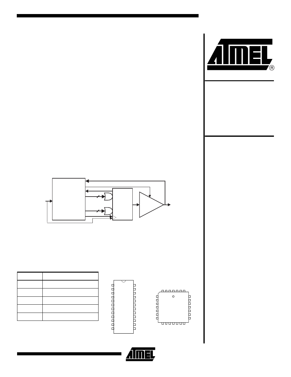
Block Diagram
Description
The ATF750C(L)s are twice as powerful as most other 24-pin programmable logic
devices. Increased product terms, sum terms, flip-flops and output logic configurations
translate into more usable gates. High-speed logic and uniform predictable delays
PROGRAMMABLE
INTERCONNECT
AND
COMBINATORIAL
LOGIC ARRAY
LOGIC
OPTION
(UP T0 20
FLIP-FLOPS)
OUTPUT
OPTION
4 TO 8
PRODUCT
TERMS
(OE PRODUCT TERMS)
10
I/O
PINS
12
INPUT
PINS
(CLOCK PIN)
Rev. 0776H–03/01
High-speed
Complex
Programmable
Logic Device
ATF750C
ATF750CL
Pin Configurations
Pin Name
Function
CLK
Clock
IN
Logic Inputs
I/O
Bi-directional Buffers
GND
Ground
VCC
+5V Supply
(continued)
DIP/SOIC/TSSOP
1
2
3
4
5
6
7
8
9
10
11
12
24
23
22
21
20
19
18
17
16
15
14
13
CLK/IN
IN
IN
IN
IN
IN
IN
IN
IN
IN
IN
GND
VCC
I/O
I/O
I/O
I/O
I/O
I/O
I/O
I/O
I/O
I/O
IN
PLCC
5
6
7
8
9
10
11
25
24
23
22
21
20
19
IN
IN
IN
GND *
IN
IN
IN
I/O
I/O
I/O
GND *
I/O
I/O
I/O
4
3
2
1
28
27
26
12
13
14
15
16
17
18
IN
IN
GND
GND *
IN
I/O
I/O
IN
IN
CLK/IN
VCC *
VCC
I/O
I/O
Note:
For PLCC, pins 1, 8, 15, and 22
can be left unconnected. For
superior performance, connect
VCC to pin 1 and GND to pins
8, 15, and 22.
Document Outline
- Features
- Block Diagram
- Description
- Absolute Maximum Ratings*
- DC and AC Operating Conditions
- Logic Options
- Clock Mux
- Output Options
- Bus-friendly Pin-keeper Input and I/Os
- Input Diagram
- I/O Diagram
- DC Characteristics
- Input Test Waveforms and Measurement Levels
- Output Test Load
- AC Waveforms, Product Term Clock(1)
- AC Characteristics, Product Term Clock(1)
- AC Waveforms, Input Pin Clock(1)
- AC Characteristics, Input Pin Clock
- Functional Logic Diagram ATF750C, Upper Half
- Functional Logic Diagram ATF750C, Lower Half
- Preload of Registered Outputs
- Power-up Reset
- Pin Capacitance
- Using the ATF750C’s Many Advanced Features
- Synchronous Preset and Asynchronous Reset
- Security Fuse Usage
- Pin Configurations
- ATF750C(L) Ordering Information
- Using “C” Product for Industrial