Ds3501 high-voltage, nv, i, C pot with temp sensor and lookup table – Rainbow Electronics DS3501 User Manual
Page 8
DS3501
High-Voltage, NV, I
2
C POT with Temp Sensor
and Lookup Table
8
_____________________________________________________________________
LUT Mode
LUT Mode is selected by setting the Update Mode bit
(CR1.0) to 1 and the Adder Mode bit (CR1.1) to 0. An
overview of the DS3501 in this mode is illustrated in the
LUT Mode and LUT Adder Mode Block Diagram. Also,
the memory map for LUT Mode and LUT Adder Mode is
shown in Table 3. The major difference between the two
LUT modes is whether or not the value in the IVR is
added to the values stored in the lookup table. The
dashed line/arrow shown in the block diagram is not
active in LUT mode.
When in LUT Mode, on power-up the IVR value is
recalled into the WR register. This value will remain
there until completion of the first temperature conver-
sion following power-up. The temperature is measured
every t
FRAME
. The temperature value is used to calcu-
late an index that points to the corresponding value in
the lookup table. This index is referred to as the LUT
Address Register (LUTAR). The value stored in the LUT
at the location pointed to by LUTAR is called LUTVAL.
The Wiper Register is then automatically loaded with
LUTVAL. The process then repeats itself, continuously
updating the wiper setting in a closed-loop fashion.
In this mode the 36-byte LUT is populated with wiper
settings for each four-degree temperature window.
Valid wiper settings are 00h to 7Fh. The memory map in
Table 3 shows the memory address of the LUT as well
as the corresponding temperature range for each byte
in the LUT. Also, the LUT features one-degree hystere-
sis to prevent chattering if the measured temperature
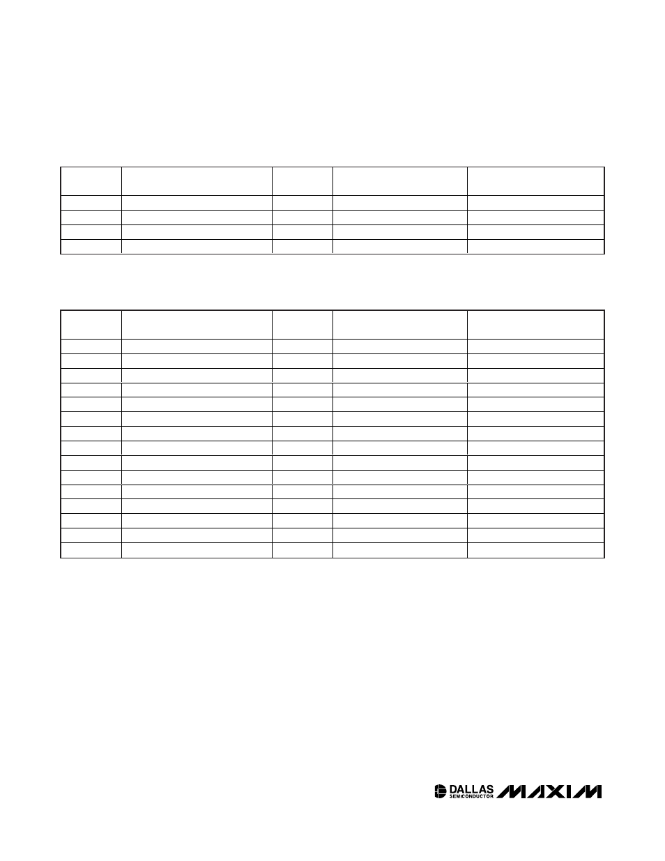
REGISTER
NAME
ADDRESS
(HEX)
VOLATILE/NONVOLATILE
FACTORY/POWER-UP
DEFAULT
WR/IVR
Wiper Register/Initial Value
00h*
NV (Shadowed)
40h
CR0
Control Register 0
02h
V
00h
CR1
Control Register 1
03h
NV (Shadowed)
00h
CR2
Control Register 2
0Ah
V
00h
Table 2. Default Mode Memory Map
*
In Default Mode, both WR and IVR are accessed through memory location 00h. Refer to the Default Mode section for additional information.
REGISTER
NAME
ADDRESS
(HEX)
VOLATILE/NONVOLATILE
FACTORY/POWER-UP
DEFAULT
IVR
Initial Value Register
00h*
NV (Shadowed)
40h
CR0
Control Register 0
02h
V
00h
CR1
Control Register 1
03h
NV (Shadowed)
00h
LUTAR
LUT Address Register
08h
V
N/A
WR
Wiper Register
09h*
V
N/A
CR2
Control Register 2
0Ah
V
00h
TEMP
Temperature Value
0Ch
V (Read-Only)
N/A
VCC
V
CC
Voltage Value
0Eh
V (Read-Only)
N/A
LUT0
Wiper Value for T
≤ -37°C
80h
NV
00h
LUT1
Wiper Value for -36°C to -33°C
81h
NV
00h
LUT2
Wiper Value for -32°C to -29°C
82h
NV
00h
—
—
—
—
—
LUT33
Wiper Value for +92°C to +95°C
A1h
NV
00h
LUT34
Wiper Value for +96°C to +99°C
A2h
NV
00h
LUT35
Wiper Value for T
≥ 100°C
A3h
NV
00h
Table 3. LUT Mode and LUT Adder Mode Memory Map
*
In LUT Mode and LUT Adder Mode, the WR is accessed through memory address 09h, while IVR remains at memory address 00h.