Ds3501 high-voltage, nv, i, C pot with temp sensor and lookup table, C serial interface description – Rainbow Electronics DS3501 User Manual
Page 10
DS3501
High-Voltage, NV, I
2
C POT with Temp Sensor
and Lookup Table
10
____________________________________________________________________
Standby Mode and I
CC
The DS3501 has three specified levels of supply cur-
rent. Active current during I
2
C communications while in
the LUT-driven mode is specified as I
CC
, and is the
“worst-case” supply current. Active current without I
2
C
communications while in the LUT driven mode is speci-
fied as the supply current: I
CC2
. SDA and SCL are held
statically in the high-logic level while the DS3501 con-
tinues to function in LUT-driven mode. The third level is
specified as standby mode, I
STBY
. This is the lowest
possible current consumption mode.
Standby mode is enabled with CR2.0 = 1. All internal
operations are halted including internal temperature
sensor results. Consequently, WR’s position will not
change, and will remain in the last state that was
loaded into WR. I
2
C will, however, continue to function,
and once CR2.0 = 0, the DS3501 will resume normal
operation after the first temperature conversion cycle is
complete (t
FRAME
).
Slave Address Byte and Address Pins
The slave address byte consists of a 7-bit slave
address plus a R/W bit (see Figure 2). The DS3501’s
slave address is determined by the state of the A0 and
A1 address pins. These pins allow up to four devices to
reside on the same I
2
C bus. Address pins tied to GND
result in a 0 in the corresponding bit position in the
slave address. Conversely, address pins tied to V
CC
result in a 1 in the corresponding bit positions. For
example, the DS3501’s slave address byte is 50h when
A0 and A1 pins are grounded. I
2
C communication is
described in detail in the
I
2
C Serial Interface
Description
section.
I
2
C Serial Interface Description
I
2
C Definitions
The following terminology is commonly used to describe
I
2
C data transfers. (See Figure 3 and
I
2
C AC Electrical
Characteristics
table for additional information.)
Master device: The master device controls the slave
devices on the bus. The master device generates SCL
clock pulses and START and STOP conditions.
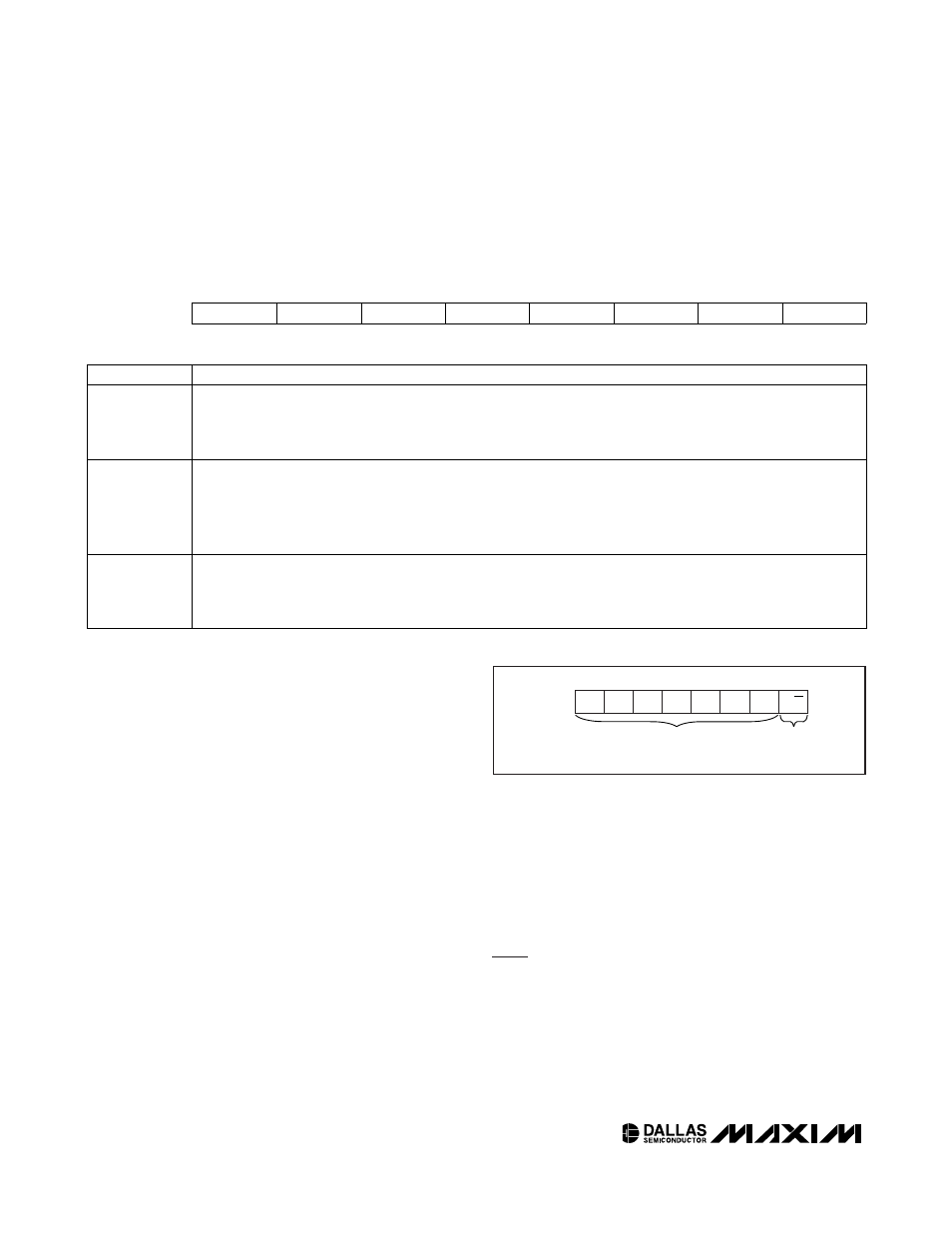
Control Register 2 (CR2)
POWER-UP DEFAULT
00h
MEMORY TYPE
Volatile
0Ah
Reserved
Reserved
Reserved
Reserved
Reserved
TEN
AEN
Standby
bit7
bit0
bit7:3
Reserved
bit2
TEN: Temperature Update Enable bar. This bit is valid only in LUT Mode and LUT Adder Mode.
0 = Normal LUT operation. The WR is automatically loaded with LUTVAL+IVR or LUTVAL following each
temperature conversion.
1 = Places the potentiometer in manual mode allowing WR (09h) to be written using I
2
C.
bit1
AEN: Address Update Enable bar. This bit is valid only in LUT Mode and LUT Adder Mode.
0 = Normal LUT operation. LUTAR (08h) is calculated following each temperature conversion that points to the
corresponding location in the LUT.
1 = Disables automatic updates of LUTAR. This allow the user to directly write to the LUTAR register in order to
exercise LUT values and functionality.
bit0
Standby:
0 = Normal operating mode.
1 = Standby Mode. Places the DS3501 in a low-power consumption state specified by I
STBY
. The I
2
C interface
is still active in this state.
0
1
1
0
R/W
A0
A1
0
MSB
LSB
SLAVE ADDRESS*
*THE SLAVE ADDRESS IS DETERMINED BY ADDRESS PINS A0, A1.
Figure 2. DS3501 Slave Address Byte