Ds3501 high-voltage, nv, i, C pot with temp sensor and lookup table, C ac electrical characteristics (continued) – Rainbow Electronics DS3501 User Manual
Page 4
DS3501
High-Voltage, NV, I
2
C POT with Temp Sensor
and Lookup Table
4
_____________________________________________________________________
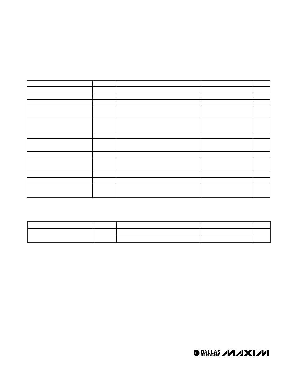
NONVOLATILE MEMORY CHARACTERISTICS
(V
CC
= +2.7V to +5.5V)
PARAMETER
SYMBOL
CONDITIONS
MIN
TYP
MAX
UNITS
T
A
= +70°C
50,000
EEPROM Write Cycles
T
A
= +25°C
200,000
Writes
Note 1: All voltages are referenced to ground. Currents entering the IC are specified positive and currents exiting the IC are nega-
tive.
Note 2: I
CC
is specified with the following conditions: SCL = 400kHz; SDA pulled up; and RL, RW, RH floating.
Note 3: I
CC
is specified with the following conditions: SCL, SDA pulled up; RL, RW, RH floating; and temperature sensor on.
Note 4: I
STBY
is specified with SDA = SCL = V
CC
= 5.5V, resistor pins floating, and CR2 bit 0 = logic-high.
Note 5: This is the minimum V
CC
voltage that causes NV memory to be recalled.
Note 6: This is the time from V
CC
> V
POR
until initial memory recall is complete.
Note 7: Guaranteed by design.
Note 8: Integral nonlinearity is the deviation of a measured resistor setting value from the expected values at each particular resis-
tor setting. Expected value is calculated by connecting a straight line from the measured minimum setting to the measured
maximum setting. INL = [V(RW)
i
- (V(RW)
0
] / LSB(ideal) - i, for i = 0...127.
Note 9: Differential nonlinearity is the deviation of the step-size change between two LSB settings from the expected step size. The
expected LSB step size is the slope of the straight line from measured minimum position to measured maximum position.
DNL = [V(RW)
i+1
- (V(RW)
i
] / LSB(ideal) - 1, for i = 0...126.
Note 10: ZS error = code 0 wiper voltage divided by one LSB(ideal).
Note 11: FS error = (code 127 wiper voltage - V+) divided by one LSB (ideal).
Note 12: I
2
C interface timing shown is for fast-mode (400kHz) operation. This device is also backward-compatible with I
2
C standard
mode timing.
Note 13: CB—total capacitance of one bus line in picofarads.
Note 14: EEPROM write time begins after a STOP condition occurs.
Note 15: Pulses narrower than max are suppressed.
I
2
C AC ELECTRICAL CHARACTERISTICS (continued)
(V
CC
= +2.7V to +5.5V, T
A
= -40°C to +100°C, timing referenced to V
IL(MAX)
and V
IH(MIN)
. See Figure 3.)
PARAMETER
SYMBOL
CONDITIONS
MIN
TYP
MAX
UNITS
Data Hold Time
t
HD:DAT
0
0.9
µs
Data Setup Time
t
SU:DAT
100
ns
START Setup Time
t
SU:STA
0.6
µs
SDA and SCL Rise Time
t
R
(Note 13)
20 +
0.1C
B
300
ns
SDA and SCL Fall Time
t
F
(Note 13)
20 +
0.1C
B
300
ns
STOP Setup Time
t
SU:STO
0.6
µs
SDA and SCL Capacitive
Loading
C
B
(Note 13)
400
pF
EEPROM Write Time
t
W
(Note 14)
10
20
ms
Pulse-Width Suppression Time at
SDA and SCL Inputs
t
IN
(Note 15)
50
ns
A0, A1 Setup Time
t
SU:A
Before START
0.6
µs
A0, A1 Hold Time
t
HD:A
After STOP
0.6
µs
SDA and SCL Input Buffer
Hysteresis
0.05 x
V
CC
V