Ds3501 high-voltage, nv, i, C pot with temp sensor and lookup table, Dc electrical characteristics – Rainbow Electronics DS3501 User Manual
Page 2
DS3501
High-Voltage, NV, I
2
C POT with Temp Sensor
and Lookup Table
2
_____________________________________________________________________
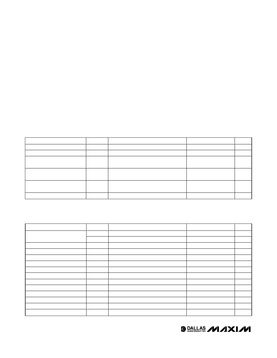
ABSOLUTE MAXIMUM RATINGS
RECOMMENDED OPERATING CONDITIONS
(T
A
= -40°C to +100°C)
Stresses beyond those listed under “Absolute Maximum Ratings” may cause permanent damage to the device. These are stress ratings only, and functional
operation of the device at these or any other conditions beyond those indicated in the operational sections of the specifications is not implied. Exposure to
absolute maximum rating conditions for extended periods may affect device reliability.
Voltage Range on V
CC
Relative to GND ...............-0.5V to +6.0V
Voltage Range on V+ Relative to GND ..................-0.5V to +17V
Voltage Range on SDA, SCL, A0, A1
Relative to GND..........-0.5V to (V
CC
+ 0.5V), not to exceed 6.0V
Voltage Range on RH, RL, RW...................................-0.5V to V+
Voltage Range Across RH and RL Pins .....................-0.5V to V+
Operating Temperature Range .........................-40°C to +100°C
Programming Temperature Range .........................0°C to +70°C
Storage Temperature Range .............................-55°C to +125°C
Soldering Temperature .......................................See IPC/JEDEC
J-STD-020 Specification
Maximum RW Current ...........................................................1mA
PARAMETER
SYMBOL
CONDITIONS
MIN
TYP
MAX
UNITS
Supply Voltage
V
CC
(Note 1)
+2.7
+5.5
V
V+ Voltage
V+
V+ > V
CC
+4.5
+15.5
V
Input Logic 1
(SCL, SDA, A0, A1)
V
IH
0.7 x
V
CC
V
CC
+ 0.3
V
Input Logic 0
(SCL, SDA, A0, A1)
V
IL
-0.3
0.3 x
V
CC
V
Resistor Inputs (RL, RW, RH)
V
RES
-0.3
V+
+ 0.3
V
Wiper Current
I
WIPER
1
mA
DC ELECTRICAL CHARACTERISTICS
(V
CC
= +2.7V to +5.5V, T
A
= -40°C to +100°C, unless otherwise noted.)
PARAMETER
SYMBOL
CONDITIONS
MIN
TYP
MAX
UNITS
I
CC
(Note 2)
2
mA
V
CC
Supply Current
I
CC2
(Note 3)
250
350
µA
Standby Supply Current
I
STBY
(Note 4)
40
60
µA
V+ Bias Current
I
V+
+1
µA
Inp ut Leakag e ( S D A, S C L, A0, A1)
I
L
-1
+1
µA
Low-Level Output Voltage (SDA)
V
OL
3mA sink current
0.0
0.4
V
I/O Capacitance
C
I/O
5
10
pF
Power-Up Recall Voltage
V
POR
(Note 5)
1.6
2.6
V
Power-Up Memory Recall Delay
t
D
(Note 6)
5
ms
Wiper Resistance
R
W
V+ = 15.0V
5000
Ω
E nd - to- E nd Resi stance ( RH to RL)
R
TOTAL
10
k
Ω
R
TOTAL
Tolerance
T
A
= +25°C
-20
+20
%
R
TOTAL
Temp Co.
(Note 7)
±200
ppm
CH, CL, CW Capacitance
C
POT
10
pF