Ds3501 high-voltage, nv, i, C pot with temp sensor and lookup table, Applications information – Rainbow Electronics DS3501 User Manual
Page 13: Chip information, Power-supply decoupling, Sda and scl pullup resistors, C ac electrical characteristics
DS3501
High-Voltage, NV, I
2
C POT with Temp Sensor
and Lookup Table
____________________________________________________________________
13
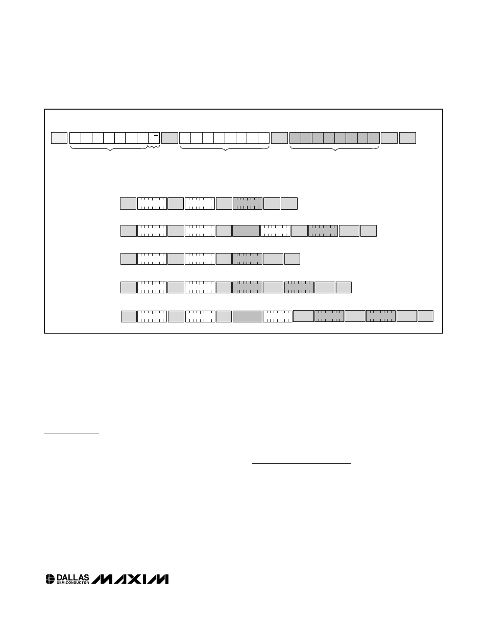
Reading multiple bytes from a slave: The read opera-
tion can be used to read multiple bytes with a single
transfer. When reading bytes from the slave, the master
simply ACKs the data byte if it desires to read another
byte before terminating the transaction. After the master
reads the last byte it must NACK to indicate the end of
the transfer and generates a STOP condition.
Applications Information
Power-Supply Decoupling
To achieve the best results when using the DS3501,
decouple both the power-supply pin and the wiper-bias
voltage pin with a 0.01µF or 0.1µF capacitor. Use a
high-quality ceramic surface-mount capacitor if possi-
ble. Surface-mount components minimize lead induc-
tance, which improves performance, and ceramic
capacitors tend to have adequate high-frequency
response for decoupling applications.
SDA and SCL Pullup Resistors
SDA is an I/O with an open-collector output that
requires a pullup resistor to realize high-logic levels. A
master using either an open-collector output with a
pullup resistor or a push-pull output driver can be used
for SCL. Pullup resistor values should be chosen to
ensure that the rise and fall times listed in the
I
2
C AC
Electrical Characteristics
are within specification. A typ-
ical value for the pullup resistors is 4.7k
Ω.
Chip Information
TRANSISTOR COUNT: 22,400
SUBSTRATE CONNECTED TO GROUND
SLAVE
ADDRESS*
START
START
0
1
0
1
0
A1
A0
R/W
SLAVE
ACK
SLAVE
ACK
SLAVE
ACK
MSB
LSB
MSB
LSB
MSB
LSB
b7
b6
b5
b4
b3
b2
b1
b0
READ/
WRITE
REGISTER ADDRESS
b7
b6
b5
b4
b3
b2
b1
b0
DATA
STOP
SINGLE-BYTE WRITE
-WRITE LUTAR
REGISTER TO 00h
SINGLE-BYTE WRITE
SET TO LUT MODE
SINGLE-BYTE READ
-READ CR0 REGISTER
TWO-BYTE WRITE
- WRITE 80h AND 81h TO 00h
START
REPEATED
START
51h
MASTER
NACK
STOP
0 1 0 1 0 0 0 0
0 0 0 0 0 0 1 0
02h
0 1 0 1 0 0 0 1
0 1 0 1 0 0 0 0
0 0 0 0 1 0 0 0
50h
08h
STOP
START 0 1 0 1 0 0 0 0
0 0 0 0 0 0 1 1
50h
CR1 (03h)
STOP
DATA
01h
EXAMPLE I
2
C TRANSACTIONS (WHEN A0 AND A1 ARE CONNECTED TO GND).
TYPICAL I
2
C WRITE TRANSACTION
*THE SLAVE ADDRESS IS DETERMINED BY ADDRESS PINS A0 AND A1.
0 0 0 0 0 0 0 0
0 0 0 0 0 0 0 1
50h
A)
C)
B)
D)
SLAVE
ACK
SLAVE
ACK
SLAVE
ACK
SLAVE
ACK
SLAVE
ACK
SLAVE
ACK
SLAVE
ACK
SLAVE
ACK
SLAVE
ACK
START 0 1 0 1 0 0 0 0
1 0 0 0 0 0 0 0
50h
80h
STOP
00h
0 0 0 0 0 0 0 0
SLAVE
ACK
SLAVE
ACK
SLAVE
ACK
00h
0 0 0 0 0 0 0 0
SLAVE
ACK
TWO-BYTE READ
- READ 80h AND 81H
E)
START 0 1 0 1 0 0 0 0
1 0 0 0 0 0 0 0
50h
80h
STOP
SLAVE
ACK
SLAVE
ACK
SLAVE
ACK
MASTER
ACK
51h
0 1 0 1 0 0 0 1
DATA
DATA
MASTER
ACK
LUT 1
LUT 0
REPEATED
START
Figure 4. I
2
C Communication Examples