Rainbow Electronics DS89C450 User Manual
Page 31
DS89C430/DS89C440/DS89C450 Ultra-High-Speed Flash Microcontrollers
31 of 48
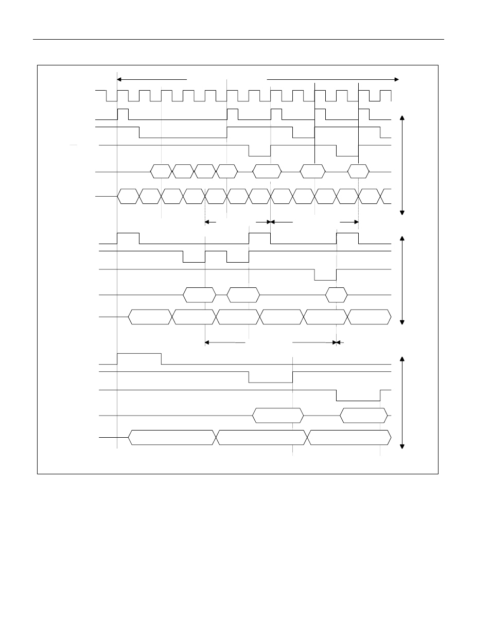
Figure 10. Page Mode 1, External Memory Cycle (CD1:CD0 = 10)
Internal Memory Cycles
XTAL1
ALE
Port 0
Port 2
Data
Data
Inst
MSB
MSB
MSB
MSB
MSB
LSB
LSB
LSB
LSB
LSB
LSB
Inst
Inst
External Memory Cycles
Page Miss
Page Hit
Page Miss
Data Access
Data Access
PAGES=00
ALE
PSEN
MOVX
Inst
Data
Page Miss
Page Miss
Data Access
Page Hit
MSBAdd
LSB Add
LSB Add
MSBAdd
MSBAdd
LSB Add
PAGES=01
Port 0
Port 2
MSBAdd
LSB Add
LSB Add
Inst
Data
Port 2
Port 0
PSEN
ALE
Page Miss
Data Access
RD/WR
RD/WR
PAGES=10
RD/WR
MOVX MOVX
LSB
PSEN
MOVX executed
MOVX executed
MOVX executed
next instruction
During a page miss, P2 drives the Addr [8:15] of the 16-bit address and holds it for the duration of the first half of
the memory cycle to allow the external address latches to latch the new most significant address byte. ALE is
asserted to strobe the external address latches. During this operation,
PSEN, RD, and WR are held in inactive
states and P0 is in a high-impedance state. The following half-memory cycle is executed as a page hit cycle and
the appropriate operation takes place.
A page miss can occur at set intervals or during external operations that require a memory access into a page of
memory that has not been accessed during the last external cycle. Generally, the first external memory access
causes a page miss. The new page address is stored internally and is used to detect a page miss for the current
external memory cycle.