Absolute maximum ratings, Dc electrical characteristics – Rainbow Electronics DS89C450 User Manual
Page 2
DS89C430/DS89C44/DS89C450 Ultra-High-Speed Flash Microcontrollers
2 of 48
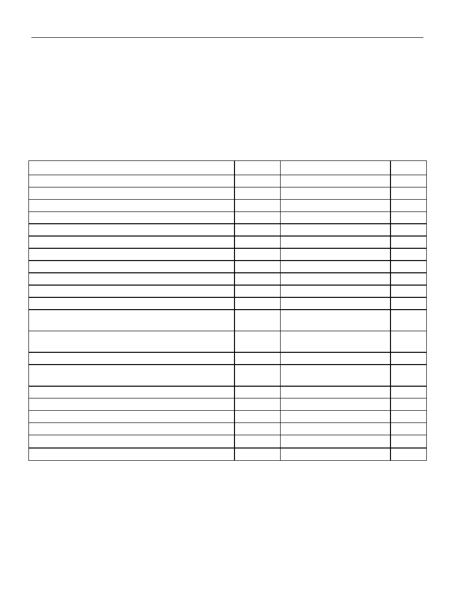
ABSOLUTE MAXIMUM RATINGS
Voltage Range on Any Pin Relative to Ground
-0.3V to (V
CC
+ 0.5V)
Voltage Range on V
CC
Relative to Ground
-0.3V to +6.0V
Ambient Temperature Range (under bias)
-40°C to +85°C
Storage Temperature Range
-55°C to +125°C
Soldering Temperature
See IPC/JEDEC J-STD-020A
Stresses beyond those listed under “Absolute Maximum Ratings” may cause permanent damage to the device. These are stress ratings only,
and functional operation of the device at these or any other conditions beyond those indicated in the operational sections of the specifications is
not implied. Exposure to the absolute maximum rating conditions for extended periods may affect device reliability.
DC ELECTRICAL CHARACTERISTICS
(V
CC
= 4.5V to 5.5V, T
O
= -40°C to +85°C.) (Note 1)
PARAMETER SYMBOL
MIN
TYP
MAX
UNITS
Supply Voltage (Notes 2, 3)
V
CC
4.5 5.0 5.5 V
Power-Fail Warning (Notes 2, 4)
V
PFW
4.2
4.375
4.6 V
Reset Trip Point (Min Operating Voltage) (Notes 2, 3, 4)
V
RST
3.95
4.125
4.35 V
Supply Current, Active Mode (Note 5)
I
CC
75
110
mA
Supply Current, Idle Mode at 33MHz (Note 6)
I
IDLE
40
50
mA
Supply Current, Stop Mode, Bandgap Disabled (Note 7)
I
STOP
1
100
mA
Supply Current, Stop Mode, Bandgap Enabled (Note 7)
I
SPBG
150
300
mA
Input Low Level (Note 2)
V
IL
-0.3 +0.8 V
Input High Level (Note 2)
V
IH
2.0
V
CC
+ 0.3
V
Input High Level XTAL and RST (Note 2)
V
IH2
3.5
V
CC
+ 0.3
V
Output Low Voltage, Port 1 and 3 at I
OL
= 1.6mA (Note 2)
V
OL1
0.15
0.45
V
Output Low Voltage, Port 0 and 2, ALE,
PSEN at I
OL
= 3.2mA
(Note 2)
V
OL2
0.15
0.45
V
Output High Voltage, Port 1, 2, and 3, at I
OH
= -50
mA
(Notes 2, 8)
V
OH1
2.4 V
Output High Voltage, Port 1, 2, and 3 at I
OH
= -1.5mA (Notes 2, 9)
V
OH2
2.4 V
Output High Voltage, Port 0, 1, 2, ALE,
PSEN, RD, WR in Bus
Mode at I
OH
= -8mA (Notes 2, 10)
V
OH3
2.4 V
Output High Voltage, RST at I
OL
= -0.4mA (Note 2, 11)
V
OH4
2.4 V
Input Low Current, Port 1, 2, and 3 at 0.4V
I
IL
-50
mA
Transition Current from 1 to 0, Port 1, 2, and 3 at 2V (Note 12)
I
TL
-650
mA
Input Leakage Current, Port 0 in I/O Mode and
EA (Note 13)
I
L
-10
+10
mA
Input Current, Port 0 in Bus Mode (Note 14)
I
L
-300
+300
mA
RST Pulldown Resistance (Note 13)
R
RST
50 120 200 k
W