Security features – Rainbow Electronics DS89C450 User Manual
Page 22
DS89C430/DS89C440/DS89C450 Ultra-High-Speed Flash Microcontrollers
22 of 48
fetch that takes four clocks. Page mode 1 is the only external addressing mode where the CPU does not require
stalls for external memory access, but page misses result in reduced external access performance.
On-Chip Program Memory
The processor can fetch the entire on-chip program memory range automatically. By default, the reset routines and
all interrupt vectors are located in the lower 128 bytes of the on-chip program memory.
On-chip program memory is logically divided into pairs of 8kB, 16kB, or 32kB flash memory banks to support in-
application programming. The on-chip program memory is designed to be programmed in-application with the
standard 5V V
CC
supply under the control of the user software or by using a built-in program memory loader. It can
also be programmed in standard flash or EPROM programmers. The DS89C430 incorporates a memory
management unit (MMU) and other hardware to support any of the three programming methods. The MMU controls
program and data memory access, and provides sequencing and timing controls for programming of the on-chip
program memory. A separate security flash block supports a standard three-level lock, a 64-byte encryption array,
and other flash options.
Security Features
The DS89C430 incorporates a 64-byte encryption array, allowing the user to verify program codes while viewing
the data in encrypted form. The encryption array is implemented in a security flash memory block that has the
same electrical and timing characteristics as the on-chip program memory. Once the encryption array is
programmed to non-FFh, the data presented in the verify mode is encrypted. Each byte of data is XNORed with a
byte in the encryption array during verification.
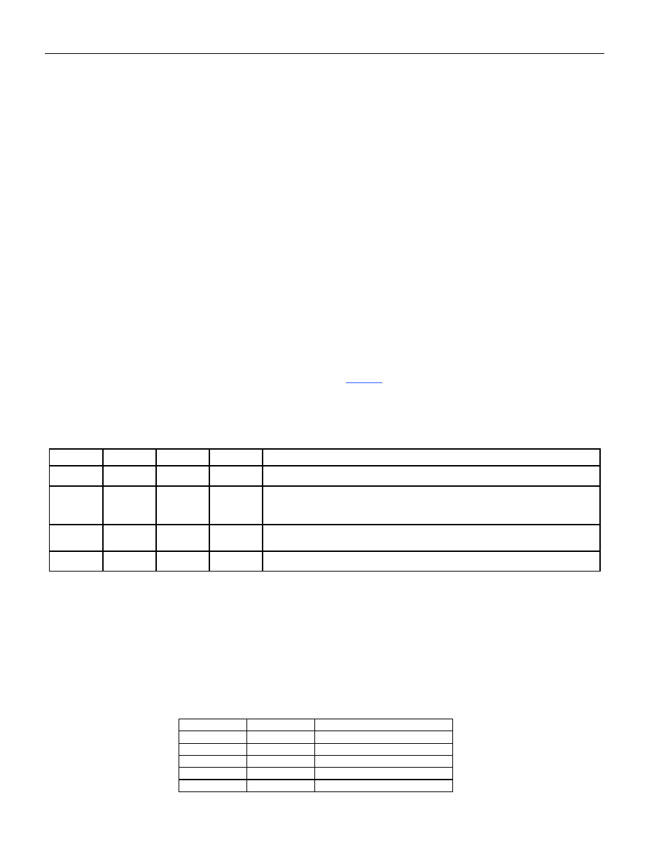
A three-level lock restricts viewing of the internal program and data memory contents. By programming the three
lock bits, the user can select a level of security as specified in
Once a security level is selected and programmed, the setting of the lock bits remains. Only a mass erase can
erase these bits and allow reprogramming the security level to a less restricted protection.
Table 3. Flash Memory Lock Bits
LEVEL LB1 LB2 LB3
PROTECTION
1
1
1
1
No program lock. Encrypted verify if encryption array is programmed.
2 0 1 1
Prevent MOVC in external memory from reading program code in internal
memory.
EA is sampled and latched on reset. Allow no further parallel or
program memory loader programming.
3 X 0 1
Level 2 plus no verify operation. Also prevent MOVX in external memory
from reading internal SRAM.
4
X
X
0
Level 3 plus no external execution.
The DS89C430 provides user-selectable options that must be set before beginning software execution. The option
control register uses flash bits rather than SFRs, and is individually erasable and programmable as a byte-wide
register. Bit 3 of this register is defined as the watchdog POR. Setting this bit to 1 disables the watchdog reset
function on power-up. Clearing this bit to 0 enables the watchdog reset function automatically. Other bits of this
register are undefined and are at logic 1 when read. The value of this register can be read at address FCh in
parallel programming mode or executing a verify-option-control register instruction in ROM loader mode or in-
application programming mode.
The signature bytes can be read in ROM loader mode or in parallel programming mode. Reading data from
addresses 30h, 31h, and 60h provides signature information on manufacturer, part, and extension as follows:
ADDRESS VALUE
MEANING
30h DAh
Manufacturer
ID
31h
43h
DS89C430 Device ID
31h
44h
DS89C440 Device ID
31h
45h
DS89C450 Device ID
60h 01h
Device
Extension