Pin description, Port 0, Port 1 – Rainbow Electronics AT89C51RC User Manual
Page 3: Port 2, Port 3, Ale/prog, At89c51rc

AT89C51RC
3
The AT89C51RC provides the following standard features:
32K bytes of Flash, 512 bytes of RAM, 32 I/O lines, three
16-bit timer/counters, a six-vector two-level interrupt archi-
tecture, a full duplex serial port, on-chip oscillator, and
clock circuitry. In addition, the AT89C51RC is designed
with static logic for operation down to zero frequency and
supports two software selectable power saving modes. The
Idle Mod e st ops t he CPU wh ile allow ing th e RAM ,
timer/counters, serial port, and interrupt system to continue
functioning. The Power-down mode saves the RAM con-
tents but freezes the oscillator, disabling all other chip func-
tions until the next external interrupt or hardware reset.
Pin Description
VCC
Supply voltage.
GND
Ground.
Port 0
Port 0 is an 8-bit open drain bidirectional I/O port. As an
output port, each pin can sink eight TTL inputs. When 1s
are written to port 0 pins, the pins can be used as high-
impedance inputs.
Port 0 can also be configured to be the multiplexed low-
order address/data bus during accesses to external
program and data memory. In this mode, P0 has internal
pull-ups.
Port 0 also receives the code bytes during Flash program-
ming and outputs the code bytes during program verifica-
tion. External pull-ups are required during program
verification.
Port 1
Port 1 is an 8-bit bidirectional I/O port with internal pull-ups.
The Port 1 output buffers can sink/source four TTL inputs.
When 1s are written to Port 1 pins, they are pulled high by
the internal pull-ups and can be used as inputs. As inputs,
Port 1 pins that are externally being pulled low will source
current (I
IL
) because of the internal pull-ups.
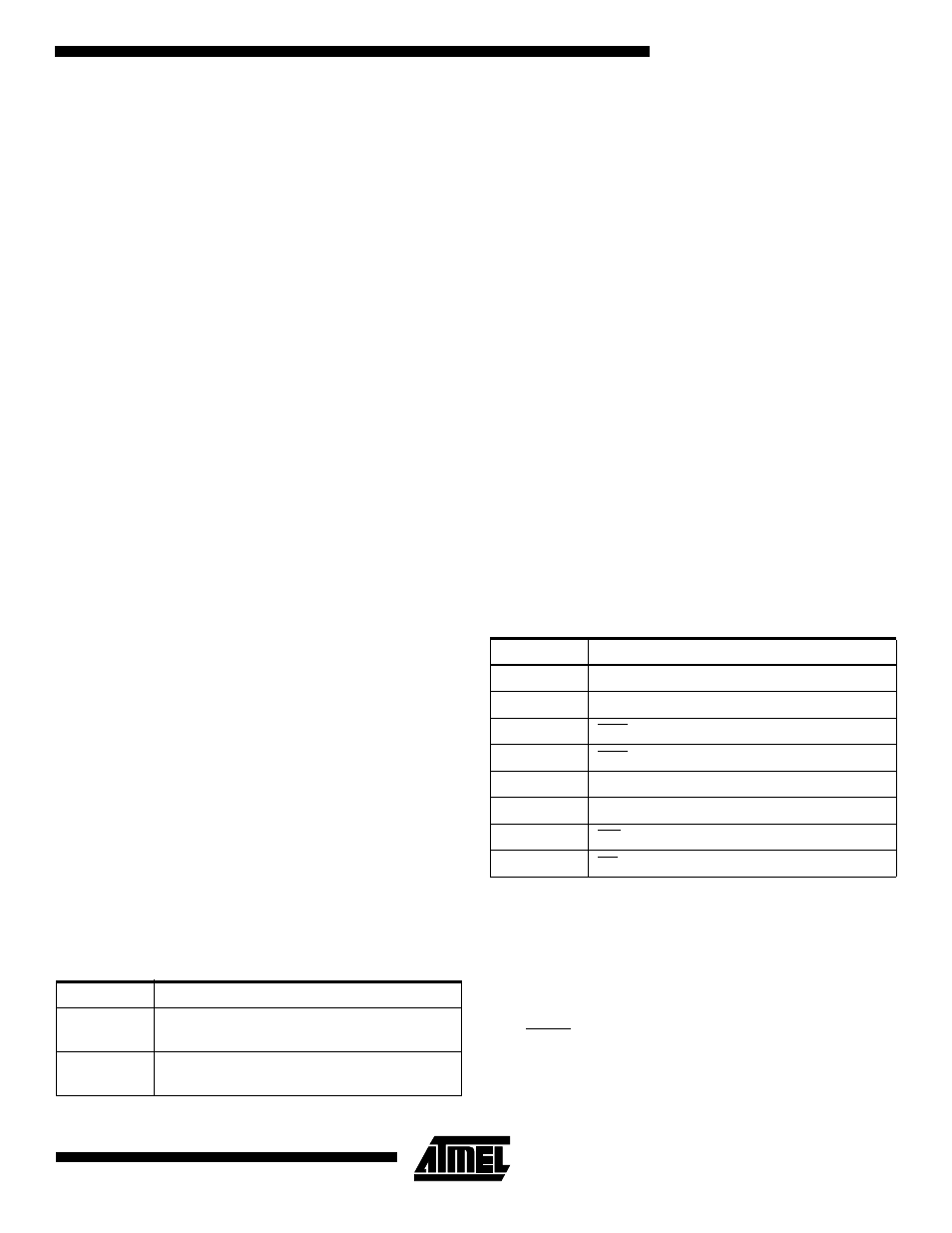
In addition, P1.0 and P1.1 can be configured to be the
timer/counter 2 external count input (P1.0/T2) and the
timer/counter 2 trigger input (P1.1/T2EX), respectively, as
shown in the following table.
Port 1 also receives the low-order address bytes during
Flash programming and verification.
Port 2
Port 2 is an 8-bit bidirectional I/O port with internal pull-ups.
The Port 2 output buffers can sink/source four TTL inputs.
When 1s are written to Port 2 pins, they are pulled high by
the internal pull-ups and can be used as inputs. As inputs,
Port 2 pins that are externally being pulled low will source
current (I
IL
) because of the internal pull-ups.
Port 2 emits the high-order address byte during fetches
from external program memory and during accesses to
external data memory that use 16-bit addresses (MOVX @
DPTR). In this application, Port 2 uses strong internal pull-
ups when emitting 1s. During accesses to external data
memory that use 8-bit addresses (MOVX @ RI), Port 2
emits the contents of the P2 Special Function Register.
Port 2 also receives the high-order address bits and some
control signals during Flash programming and verification.
Port 3
Port 3 is an 8-bit bidirectional I/O port with internal pull-ups.
The Port 3 output buffers can sink/source four TTL inputs.
When 1s are written to Port 3 pins, they are pulled high by
the internal pull-ups and can be used as inputs. As inputs,
Port 3 pins that are externally being pulled low will source
current (I
IL
) because of the pull-ups.
Port 3 also serves the functions of various special features
of the AT89C51RC, as shown in the following table.
Port 3 also receives some control signals for Flash pro-
gramming and verification.
RST
Reset input. A high on this pin for two machine cycles while
the oscillator is running resets the device. This pin drives
High for 96 oscillator periods after the Watchdog times out.
The DISRTO bit in SFR AUXR (address 8EH) can be used
to disable this feature. In the default state of bit DISTRO,
the RESET HIGH out feature is enabled.
ALE/PROG
Address Latch Enable is an output pulse for latching the
low byte of the address during accesses to external
Port Pin
Alternate Functions
P1.0
T2 (external count input to Timer/Counter 2),
clock-out
P1.1
T2EX (Timer/Counter 2 capture/reload trigger
and direction control)
Port Pin
Alternate Functions
P3.0
RXD (serial input port)
P3.1
TXD (serial output port)
P3.2
INT0 (external interrupt 0)
P3.3
INT1 (external interrupt 1)
P3.4
T0 (timer 0 external input)
P3.5
T1 (timer 1 external input)
P3.6
WR (external data memory write strobe)
P3.7
RD (external data memory read strobe)
