Programming interface, At89c51rc, Table 9. flash programming modes – Rainbow Electronics AT89C51RC User Manual
Page 16
AT89C51RC
16
Programming Interface
Every code byte in the Flash array can be programmed by
using the appropriate combination of control signals. The
write operation cycle is self-timed and once initiated, will
automatically time itself to completion.
All major programming vendors offer worldwide support for
the Atmel microcontroller series. Please contact your local
programming vendor for the appropriate software revision.
Notes:
1. Write Code Data requires a 200 ns PROG pulse.
2. Write Lock Bits requires a 100 µs PROG pulse.
3. Chip Erase requires a 200 ns - 500 ns PROG pulse.
4. RDY/BSY signal is output on P3.0 during programming.
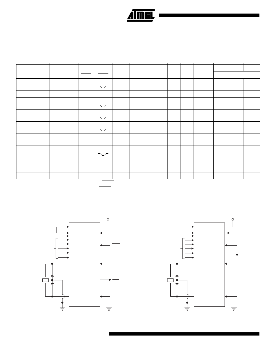
Figure 10. Programming the Flash Memory
Figure 11. Verifying the Flash Memory
Note:
*Programming address line A14 (P3.4) is not the same as the external memory address line A14 (P2.6).
Table 9. Flash Programming Modes
Mode
V
CC
RST
PSEN
ALE/
PROG
EA/
V
PP
P2.6
P2.7
P3.3
P3.6
P3.7
P0.7-0
Data
P3.4
P2.5-0
P1.7-0
Address
Write Code Data
5 V
H
L
12 V
L
H
H
H
H
D
IN
A14
A13-8
A7-0
Read Code Data
5 V
H
L
H
H/12V
L
L
L
H
H
D
OUT
A14
A13-8
A7-0
Write Lock Bit 1
6.5 V
H
L
12 V
H
H
H
H
H
X
X
X
X
Write Lock Bit 2
6.5 V
H
L
12 V
H
H
H
L
L
X
X
X
X
Write Lock Bit 3
6.5 V
H
L
12 V
H
L
H
H
L
X
X
X
X
Read Lock Bits
1, 2, 3
5 V
H
L
H
H
H
H
L
H
L
D2, 3, 4
X
X
X
Chip Erase
6.5V
H
L
12V
H
L
H
L
L
X
X
X
X
Read Atmel ID
5 V
H
L
H
H
L
L
L
L
L
1EH
X
X
000H
Read Device ID
5 V
H
L
H
H
L
L
L
L
L
51H
X
X
100H
Read Device ID
5 V
H
L
H
H
L
L
L
L
L
07H
X
X
200H
P1.0 - P1.7
P2.6
P3.6
P2.0 - P2.5
A0 - A7
ADDR.
0000H/7FFFH
SEE FLASH
PROGRAMMING
MODES TABLE
3 - 33 MHz
A14*
P0
+5V
P2.7
PGM
DATA
PROG
V /V
IH
PP
V
IH
ALE
P3.7
XTAL2
EA
RST
PSEN
XTAL1
GND
V
CC
AT89C51RC
P3.4
P3.3
P3.0
RDY/
BSY
A8 - A13
P1.0 - P1.7
P2.6
P3.6
P2.0 - P2.5
A0 - A7
ADDR.
0000H/7FFFH
SEE FLASH
PROGRAMMING
MODES TABLE
3 - 33 MHz
P0
+5V
P2.7
PGM DATA
(USE 10K
PULL-UPS)
V
IH
V
IH
ALE
P3.7
XTAL 2
EA
RST
PSEN
XTAL1
GND
V
CC
A14*
AT89C51RC
P3.4
P3.3
A8 - A13