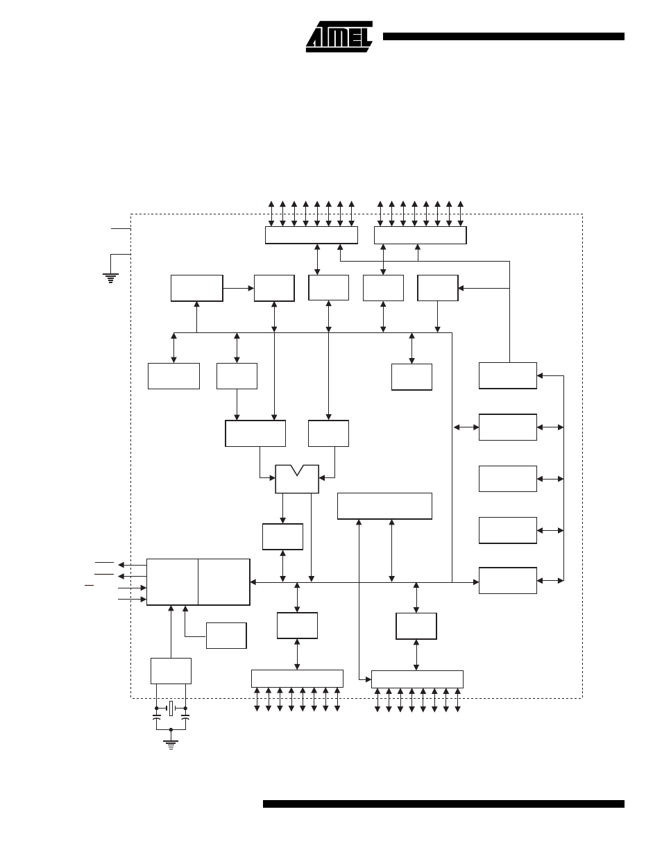
Block diagram, At89c51rc – Rainbow Electronics AT89C51RC User Manual
Page 2

AT89C51RC
2
pinout. The on-chip Flash allows the program memory to
be user programmed by a conventional nonvolatile memory
programmer. A total of 512 bytes of internal RAM are avail-
able in the AT89C51RC. The 256-byte expanded internal
RAM is accessed via MOVX instructions after clearing bit 1
in the SFR located at address 8EH. The other 256-byte
RAM segment is accessed the same way as the Atmel
AT89-series and other 8052-compatible products. By com-
bining a versatile 8-bit CPU with Flash on a monolithic chip,
the Atmel AT89C51RC is a powerful microcomputer which
provides a highly-flexible and cost-effective solution to
many embedded control applications.
Block Diagram
PORT 2 DRIVERS
PORT 2
LATCH
P2.0 - P2.7
QUICK
FLASH
PORT 0
LATCH
RAM
PROGRAM
ADDRESS
REGISTER
BUFFER
PC
INCREMENTER
PROGRAM
COUNTER
DUAL
DPTR
RAM ADDR.
REGISTER
INSTRUCTION
REGISTER
B
REGISTER
INTERRUPT, SERIAL PORT,
AND TIMER BLOCKS
STACK
POINTER
ACC
TMP2
TMP1
ALU
PSW
TIMING
AND
CONTROL
PORT 3
LATCH
PORT 3 DRIVERS
P3.0 - P3.7
PORT 1
LATCH
PORT 1 DRIVERS
P1.0 - P1.7
OSC
GND
V
CC
PSEN
ALE/PROG
EA / V
PP
RST
PORT 0 DRIVERS
P0.0 - P0.7
WATCH
DOG
