Programmable clock out, Interrupts, At89c51rc – Rainbow Electronics AT89C51RC User Manual
Page 13

AT89C51RC
13
Programmable Clock Out
A 50% duty cycle clock can be programmed to come out on
P1.0, as shown in Figure 6. This pin, besides being a regu-
lar I/O pin, has two alternate functions. It can be pro-
grammed to input the external clock for Timer/Counter 2 or
to output a 50% duty cycle clock ranging from 61 Hz to 4
MHz at a 16 MHz operating frequency.
To configure the Timer/Counter 2 as a clock generator, bit
C/T2 (T2CON.1) must be cleared and bit T2OE (T2MOD.1)
must be set. Bit TR2 (T2CON.2) starts and stops the timer.
The clock-out frequency depends on the oscillator fre-
quency and the reload value of Timer 2 capture registers
(RCAP2H, RCAP2L), as shown in the following equation.
In the clock-out mode, Timer 2 roll-overs will not generate
an interrupt. This behavior is similar to when Timer 2 is
used as a baud-rate generator. It is possible to use Timer 2
as a baud-rate generator and a clock generator simulta-
neously. Note, however, that the baud-rate and clock-out
frequencies cannot be determined independently from one
another since they both use RCAP2H and RCAP2L.
Interrupts
The AT89C51RC has a total of six interrupt vectors: two
external interrupts (INT0 and INT1), three timer interrupts
(Timers 0, 1, and 2), and the serial port interrupt. These
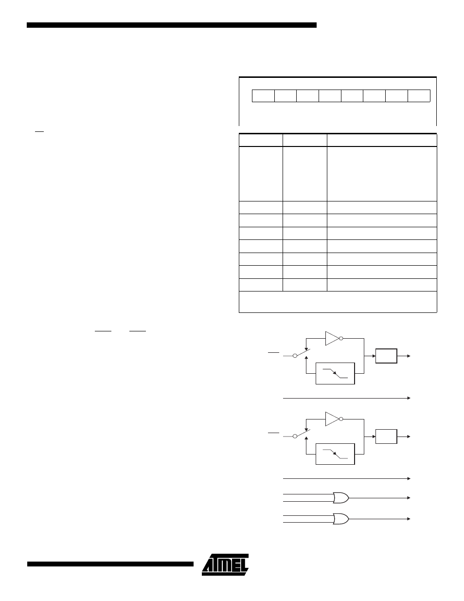
interrupts are all shown in Figure 7.
Each of these interrupt sources can be individually enabled
or disabled by setting or clearing a bit in Special Function
Register IE. IE also contains a global disable bit, EA, which
disables all interrupts at once.
Note that Table 5 shows that bit position IE.6 is unimple-
mented. In the AT89C51RC, bit position IE.5 is also unim-
plemented. User software should not write 1s to these bit
positions, since they may be used in future AT89 products.
Timer 2 interrupt is generated by the logical OR of bits TF2
and EXF2 in register T2CON. Neither of these flags is
cleared by hardware when the service routine is vectored
to. In fact, the service routine may have to determine
whether it was TF2 or EXF2 that generated the interrupt,
and that bit will have to be cleared in software.
The Timer 0 and Timer 1 flags, TF0 and TF1, are set at
S5P2 of the cycle in which the timers overflow. The values
are then polled by the circuitry in the next cycle. However,
the Timer 2 flag, TF2, is set at S2P2 and is polled in the
same cycle in which the timer overflows.
Figure 7. Interrupt Sources
Clock-Out Frequency
Oscillator Frequency
4 x [65536-(RCAP2H,RCAP2L)]
-------------------------------------------------------------------------------------
=
Table 6. Interrupt Enable (IE) Register
(MSB) (LSB)
EA
–
ET2
ES
ET1
EX1
ET0
EX0
Enable Bit = 1 enables the interrupt.
Enable Bit = 0 disables the interrupt.
Symbol
Position
Function
EA
IE.7
Disables all interrupts. If EA = 0,
no interrupt is acknowledged. If
EA = 1, each interrupt source is
individually enabled or disabled
by setting or clearing its enable
bit.
–
IE.6
Reserved.
ET2
IE.5
Timer 2 interrupt enable bit.
ES
IE.4
Serial Port interrupt enable bit.
ET1
IE.3
Timer 1 interrupt enable bit.
EX1
IE.2
External interrupt 1 enable bit.
ET0
IE.1
Timer 0 interrupt enable bit.
EX0
IE.0
External interrupt 0 enable bit.
User software should never write 1s to unimplemented bits,
because they may be used in future AT89 products.
IE1
IE0
1
1
0
0
TF1
TF0
INT1
INT0
TI
RI
TF2
EXF2
