Ata6831, Pin configuration – Rainbow Electronics ATA6831 User Manual
Page 3
3
4908D–AUTO–09/06
ATA6831
2.
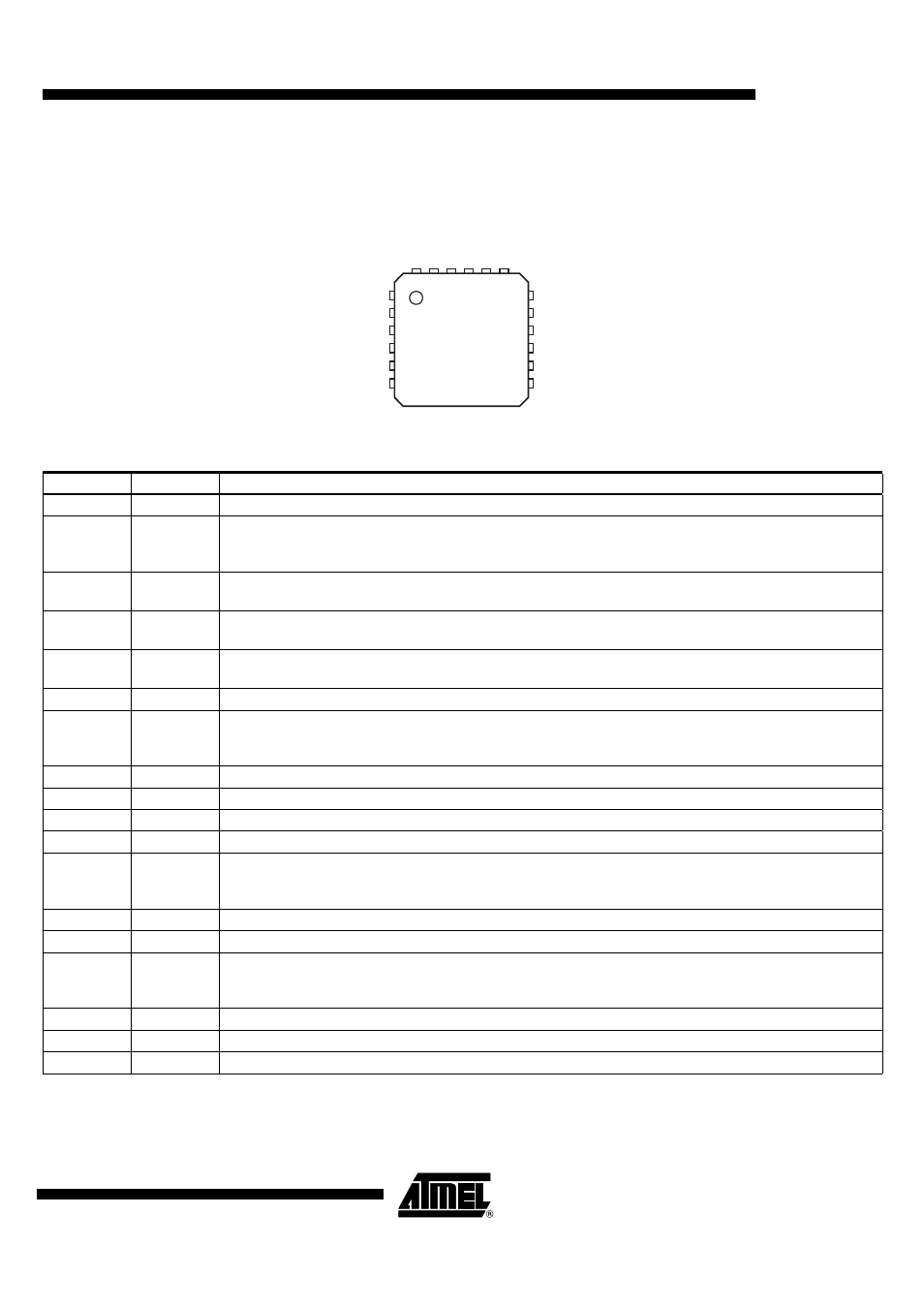
Pin Configuration
Figure 2-1.
Pinning QFN18
OUT3S
OUT3F
CS
DI
CLK
PWM
OUT2F
VS2
VS1
VCC
GND
DO
PGND3
PGND1
OUT1S
OUT1F
PGND2
OUT2S
1
2
3
4
5
6
12
11
10
9
8
7
18 17 16 15
13
14
Table 2-1.
Pin Description
Pin
Symbol
Function
1
OUT3S
Sense pin, used only for final testing
2
OUT3F
Half-bridge output 3; formed by internally connecting power MOS high-side switch 3 and low-side switch 3
with internal reverse diodes; short circuit protection; overtemperature protection; diagnosis for short and
open load
3
CS
Chip select input; 5V CMOS logic level input with internal pull-up;
low = serial communication is enabled, high = disabled
4
DI
Serial data input; 5V CMOS logic level input with internal pull-down; receives serial data from the control
device; DI expects a 16-bit control word with LSB transferred first
5
CLK
Serial clock input; 5V CMOS logic level input with internal pull-down;
controls serial data input interface and internal shift register (f
max
= 2 MHz)
6
PWM
PWM input; 5V CMOS logic level input with internal pull-down
7
DO
Serial data output; 5V CMOS logic-level tri-state output for output (status) register data; sends 16-bit status
information to the microcontroller (LSB transferred first); output will remain tri-stated unless device is
selected by CS = low; this allows several ICs to operate on only one data-output line
8
GND
Ground
9
VCC
Logic supply voltage (5V)
10
VS1
Power supply for output stages OUT1 and OUT2; internal supply
11
VS2
Power supply for output stages OUT2 and OUT3; internal supply
12
OUT2F
Half-bridge output 2; formed by internally connected power MOS high-side switch 2 and low-side switch 2
with internal reverse diodes; short circuit protection; overtemperature protection; diagnosis for short and
open load
13
OUT2S
Sense pin, used only for final testing
14
PGND2
Power ground OUT2
15
OUT1F
Half-bridge output 1; formed by internally connected power MOS high-side switch 1 and low-side switch 1
with internal reverse diodes; short circuit protection; overtemperature protection; diagnosis for short and
open load
16
OUT1S
Sense pin, used only for final testing
17
PGND1
Power ground OUT1
18
PGND3
Power ground OUT3