Rainbow Electronics ATV22V10BQL User Manual
Features, Logic diagram, Pin configurations
1
Features
•
Industry Standard Architecture
– Low-cost Easy-to-use Software Tools
•
High-speed, Electrically-erasable Programmable Logic Devices
– 7.5 ns Maximum Pin-to-pin Delay
•
Several Power Saving Options
•
CMOS and TTL Compatible Inputs and Outputs
– Input and I/O Pull-up Resistors
•
Advanced Flash Technology
– Reprogrammable
– 100% Tested
•
High-reliability CMOS Process
– 20-year Data Retention
– 100 Erase/Write Cycles
– 2,000V ESD Protection
– 200 mA Latchup Immunity
•
Full Military, Commercial, and Industrial Temperature Ranges
•
Dual-in-line and Surface Mount Packages in Standard Pinouts
•
PCI Compliant
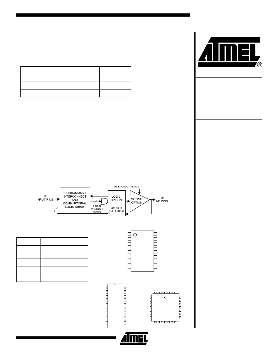
Logic Diagram
Device
I
CC
, Standby
I
CC
, Active
ATF22V10B
85 mA
90 mA
ATF22V10BQ
35 mA
40 mA
ATF22V10BQL
5 mA
20 mA
Rev. 0250K–03/01
High-
performance
EE PLD
ATF22V10B
ATF22V10BQ
ATV22V10BQL
Pin Configurations
All Pinouts Top View
Pin Name
Function
CLK
Clock
IN
Logic Inputs
I/O
Bidirectional Buffers
*
No Internal Connection
V
CC
+5V Supply
DIP/SOIC
1
2
3
4
5
6
7
8
9
10
11
12
24
23
22
21
20
19
18
17
16
15
14
13
CLK/IN
IN
IN
IN
IN
IN
IN
IN
IN
IN
IN
GND
VCC
I/O
I/O
I/O
I/O
I/O
I/O
I/O
I/O
I/O
I/O
IN
TSSOP
1
2
3
4
5
6
7
8
9
10
11
12
24
23
22
21
20
19
18
17
16
15
14
13
CLK/IN
IN
IN
IN
IN
IN
IN
IN
IN
IN
IN
GND
VCC
I/O
I/O
I/O
I/O
I/O
I/O
I/O
I/O
I/O
I/O
IN
LCC/PLCC
5
6
7
8
9
10
11
25
24
23
22
21
20
19
IN
IN
IN
*
IN
IN
IN
I/O
I/O
I/O
*
I/O
I/O
I/O
4
3
2
1
28
27
26
12
13
14
15
16
17
18
IN
IN
GND
*
IN
I/O
I/O
IN
IN
CLK/IN
*
VCC
I/O
I/O
Document Outline
- Features
- Logic Diagram
- Description
- Absolute Maximum Ratings*
- DC and AC Operating Conditions
- DC Characteristics
- AC Waveforms(1)
- AC Characteristics(1)
- Input Test Waveforms and Measurement Levels
- Output Test Loads
- Pin Capacitance
- Power-up Reset
- Preload of Registered Outputs
- Security Fuse Usage
- Electronic Signature Word
- Programming/Erasing
- Input and I/O Pull-ups
- Input Diagram
- I/O Diagram
- Functional Logic Diagram ATF22V10B
- ATF22V10B Ordering Information
- ATF22V10BQ(L) Ordering Information
- Using “C” Product for Industrial
- Pin Configurations