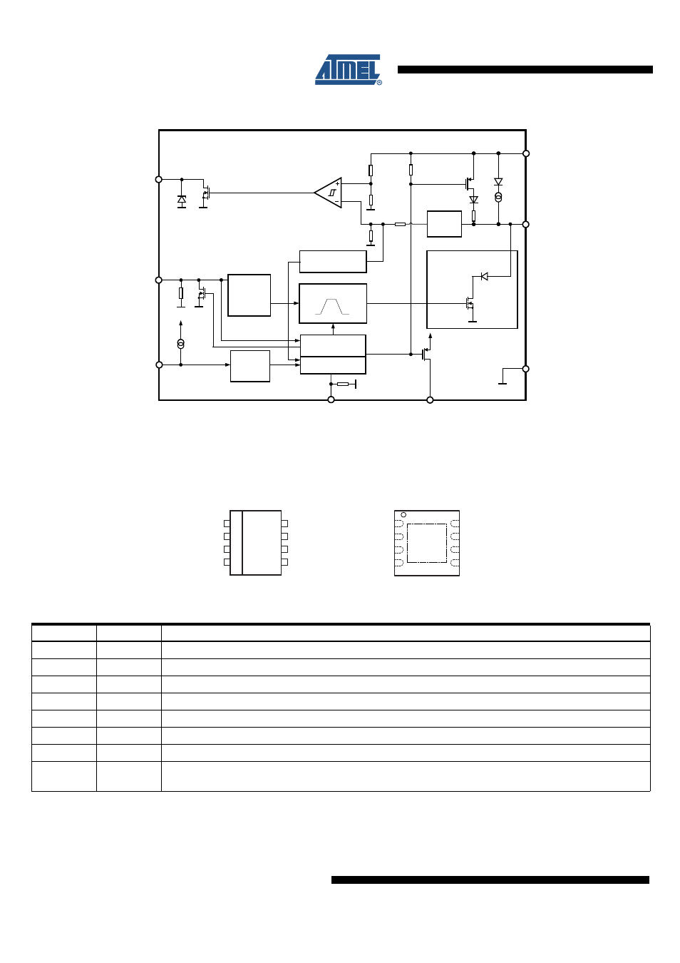
Pin configuration, Figure 1-1. block diagram, Figure 2-1. pinning so8, dfn8 – Rainbow Electronics ATA6664 User Manual
Page 2: Table 2-1. pin description

2
9146E–AUTO–03/11
Atmel ATA6663/ATA6664
Figure 1-1.
Block Diagram
2.
Pin Configuration
Figure 2-1.
Pinning SO8, DFN8
V
S
GND
5
6
LIN
7
1
4
RXD
TXD
WAKE
EN
3
2
8
INH
S
hort-circ
u
it
a
nd over-
temper
a
t
u
re protection
Receiver
Filter
W
a
ke-
u
p
bus
timer
S
lew r
a
te control
TXD
time-o
u
t
timer
V
S
W
a
ke-
u
p
timer
S
leep mode
V
S
Control
u
nit
(only ATA666
3
)
RXD
EN
WAKE
TXD
INH
V
S
LIN
GND
1
2
3
4
8
7
6
5
INH
LIN
V
S
GND
RXD
WAKE
EN
TXD
DFN8
3 x 3
SO8
Table 2-1.
Pin Description
Pin
Symbol
Function
1
RXD
Receive data output (open drain)
2
EN
Enables normal mode; when the input is open or low, the device is in sleep mode
3
WAKE
High voltage input for local wake-up request. If not needed, connect directly to VS
4
TXD
Transmit data input; active low output (strong pull-down) after a local wake-up request
5
GND
Ground, heat sink
6
LIN
LIN bus line input/output
7
VS
Battery supply
8
INH
Battery-related inhibit output for controlling an external voltage regulator or to switch-off the LIN master
pull-up resistor; active high after a wake-up request
