Detailed description – Rainbow Electronics DS4026 User Manual
Page 8
DS4026
10MHz to 51.84MHz TCXO
8
_____________________________________________________________________
DS4026
TEMP
SENSOR
V
CC
V
CC
GND
V
OSC
GNDOSC
GNDD
V
REF
V
CCD
FOUT
GNDA
SCL
SDA
I
2
C
INTERFACE
CONTROLLER
DAC
CMOS
BUFFER
A/D
GND
EEPROM
ARRAY
GND
GND
V
CC
V
CC
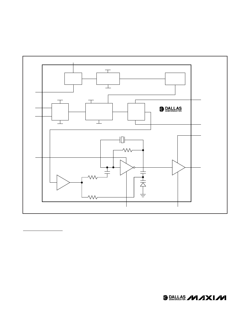
Figure 2. Functional Diagram
Detailed Description
The DS4026 is a TCXO capable of operating at 3.3V
±5%, and it allows digital tuning of the fundamental fre-
quency. The device is calibrated in the factory to
achieve an accuracy of ±1ppm over the industrial tem-
perature range, and its minimum pullability is ±8ppm
with a typical resolution of 1ppb (typ) per LSB.
The DS4026 contains the following blocks:
• Oscillator block with variable capacitor for compen-
sation
• Output driver block
• Temperature sensor
• Controller to read the temperature, control lookup
table, and adjust the DAC input
• DAC output to adjust the capacitive load
• I
2
C interface to communicate with the chip
The oscillator block consists of an amplifier and variable
capacitor in a Pierce crystal oscillator with a crystal res-
onator of fundamental mode. The oscillator amplifier is a
single transistor amplifier and its transconductance is
temperature compensated. The variable capacitor is
adjusted by the DAC to provide temperature compensa-
tion. With the FTUNEH and FTUNEL registers, a minimum
pullability of ±8ppm (±5ppm for 10MHz) is achieved with
a typical resolution of 1ppb (typ) per LSB.