Ds4026, C serial data bus, Table 1. register map – Rainbow Electronics DS4026 User Manual
Page 10
DS4026
Read Mode
In the temperature register (see the
Temperature
Register (02h–03h)
table), temperature is represented
as a 12-bit code and is accessible at location 02h and
03h. The upper 8 bits are at location 02h and the lower
4 bits are in the upper nibble of the byte at location
03h. Upon power reset, the registers are set to a +25°C
default temperature and the controller starts a tempera-
ture conversion. The temperature register stores new
temperature readings.
The current temperature is loaded into the (user) tem-
perature registers when a valid I
2
C slave address and
write is received and when a word address is received.
Consequently, if the two temperature registers are read
in individual I
2
C transactions, it is possible for a temper-
ature conversion to occur between reads, and the
results can be inaccurate. To prevent this from occur-
ring, the registers should be read using a single, multi-
byte read operation (Figure 5). I
2
C reads do not affect
the internal temperature registers.
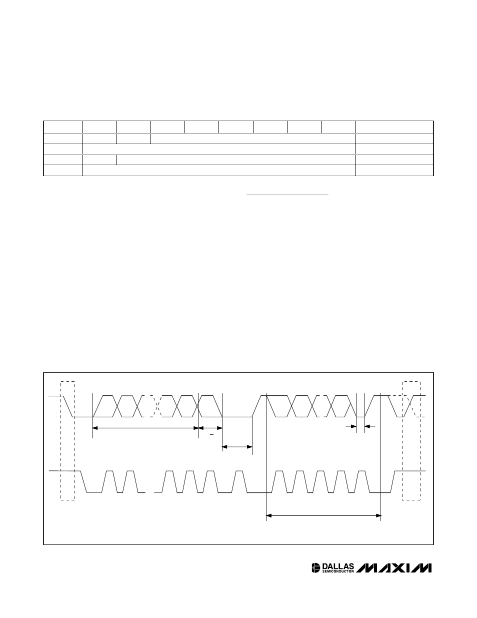
I
2
C Serial Data Bus
The DS4026 supports a bidirectional I
2
C bus and data
transmission protocol. A device that sends data onto
the bus is defined as a transmitter and a device receiv-
ing data is defined as a receiver. The device that con-
trols the message is called a master. The devices that
are controlled by the master are slaves. The bus must
be controlled by a master device that generates the
serial clock (SCL), controls the bus access, and gener-
ates the START and STOP conditions. The DS4026
operates as a slave on the I
2
C bus. Connections to the
bus are made through the open-drain I/O lines SDA
and SCL. Within the bus specifications, a standard
mode (100kHz maximum clock rate) and a fast mode
(400kHz maximum clock rate) are defined. The DS4026
works in both modes.
The following bus protocol has been defined (Figure 3):
• Data transfer can be initiated only when the bus is
not busy.
10MHz to 51.84MHz TCXO
10
____________________________________________________________________
Table 1. Register Map
ADDRESS
BIT 7
BIT 6
BIT 5
BIT 4
BIT 3
BIT 2
BIT 1
BIT 0
FUNCTION
00
DCOMP
SIGN
FTUNEH
Frequency Tuning High
01
FTUNEL
Frequency Tuning Low
02
SIGN
TREGH
Temperature MSB
03
TREGL
Temperature LSB
STOP
CONDITION
OR REPEATED
START
CONDITION
REPEATED IF MORE BYTES
ARE TRANSFERED
ACK
START
CONDITION
ACK
ACKNOWLEDGEMENT
SIGNAL FROM RECEIVER
ACKNOWLEDGEMENT
SIGNAL FROM RECEIVER
SLAVE ADDRESS
MSB
SCL
SDA
R/W
DIRECTION
BIT
1
2
6
7
8
9
1
2
8
9
3–7
Figure 3. I
2
C Data Transfer Overview