Pin description – Rainbow Electronics DS4026 User Manual
Page 7
DS4026
10MHz to 51.84MHz TCXO
_____________________________________________________________________
7
DS4026
GNDA
0.1
μF
0.1
μF
0.1
μF
20
Ω
V
REF
100
μF ±5%
CERAMIC
V
CC
V
OSC
GNDOSC
N.C.
N.C.
N.C.
V
CCD
FOUT
GNDD
SCL
SDA
GND
N.C.
N.C.
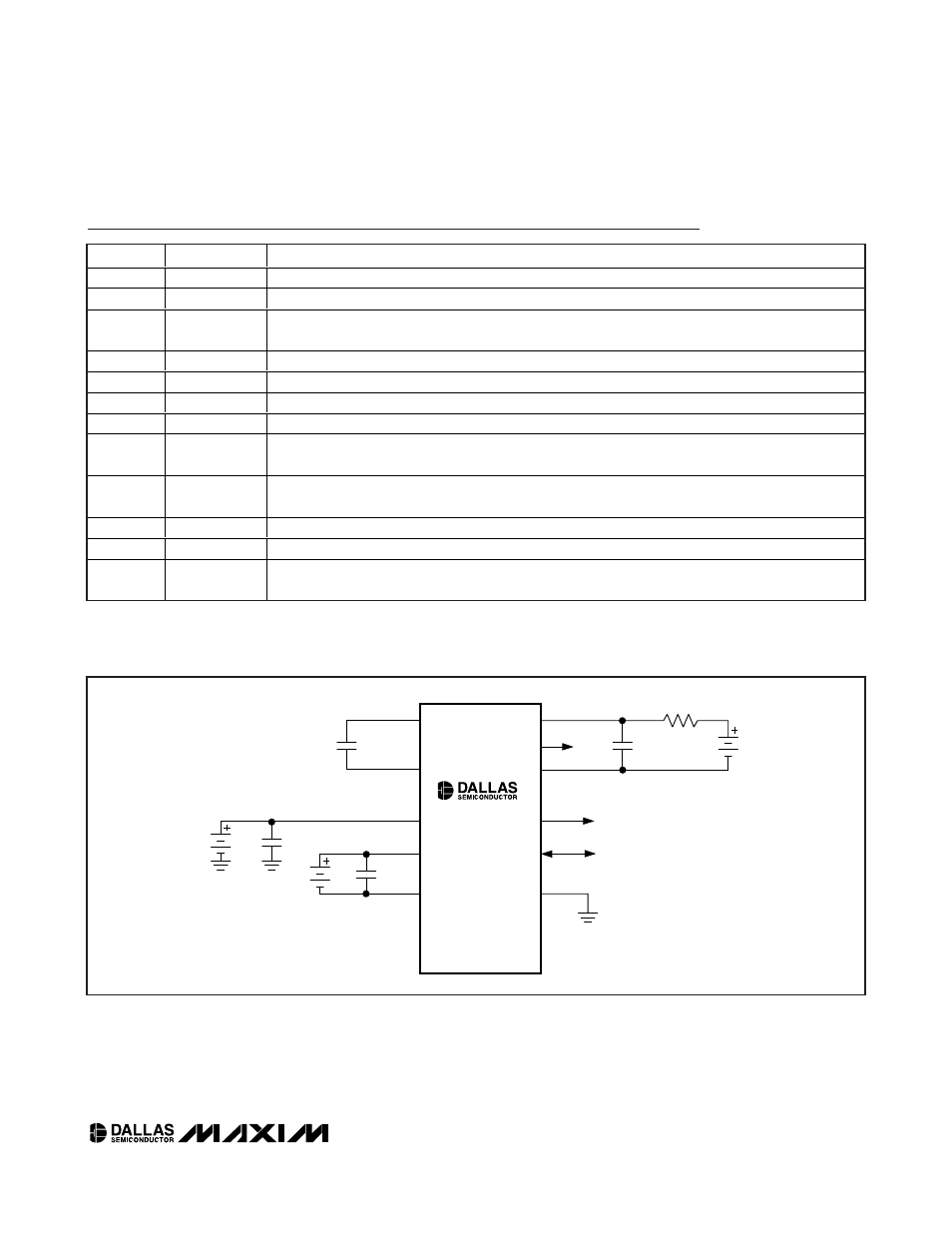
Pin Description
PIN
NAME
FUNCTION
1
GNDA
Ground for DAC
2
V
REF
Voltage Reference Output. This pin must be decoupled with a 100µF ceramic capacitor to ground.
3
V
CC
Power Supply for Digital Control and Temperature Sensor. This pin must be decoupled with a 100nF
capacitor to ground.
4
V
OSC
Power Supply for Oscillator Circuit. This pin must be decoupled with a 0.1µF capacitor to ground.
5
GNDOSC
Ground for Oscillator Circuit
6–10
N.C.
No Connection. Must be connected to ground.
11
GND
Ground for Digital Control, Temperature Sensor, and Controller Substrate
12
SDA
Serial Data Input/Output. SDA is the data input/output for the I
2
C interface. This open-drain pin
requires an external pullup resistor.
13
SCL
Serial Clock Input. SCL is the clock input for the I
2
C Interface and is used to synchronize data
movement on the serial interface.
14
GNDD
Ground for Oscillator Output Driver
15
FOUT
Frequency Output, CMOS Push-Pull
16
V
CCD
Power Supply for Oscillator Output Driver. This pin must be decoupled with a 0.1µF capacitor to
ground. A 20
Ω resistor must be placed in series between the power supply and V
CCD
.
Figure 1. Typical Operating Circuit