Rainbow Electronics DS4026 User Manual
Page 2
DS4026
10MHz to 51.84MHz TCXO
2
_____________________________________________________________________
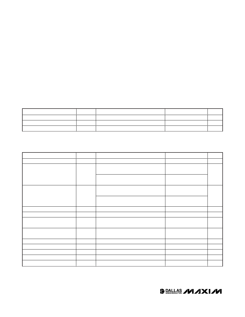
ABSOLUTE MAXIMUM RATINGS
RECOMMENDED DC OPERATING CONDITIONS
(T
A
= -40°C to +85°C, unless otherwise noted.)
Stresses beyond those listed under “Absolute Maximum Ratings” may cause permanent damage to the device. These are stress ratings only, and functional
operation of the device at these or any other conditions beyond those indicated in the operational sections of the specifications is not implied. Exposure to
absolute maximum rating conditions for extended periods may affect device reliability.
Voltage Range on V
CC
, V
CCD
, and V
OSC
Relative to Ground..............................................-0.3V to +3.8V
Voltage Range on SDA, SCL, and FOUT
Relative to Ground...................................-0.3V to (V
CC
+ 0.3V)
Operating Temperature Range (noncondensing)....-40°C to +85°C
Storage Temperature Range .............................-55°C to +125°C
Soldering Temperature………………………….See IPC/JEDEC
J-STD-020 Specification
PARAMETER
SYMBOL
CONDITIONS
MIN
TYP
MAX
UNITS
Power-Supply Voltage
V
CC
3.135
3.3
3.465
V
Oscillator Power Supply
V
OSC
3.135
3.3
3.465
V
Driver Power Supply
V
CCD
3.135
3.3
3.465
V
DC ELECTRICAL CHARACTERISTICS (Note 1)
(V
CC
= 3.135V to 3.465V, T
A
= -40°C to +85°C, unless otherwise noted.) (Notes 2, 3)
PARAMETER
SYMBOL
CONDITIONS
MIN
TYP
MAX
UNITS
V
CC
Active-Supply Current
I
CC
(Note 4)
1.5
2.5
mA
FOUT CMOS output on, CL = 10pF,
frequency < 25MHz
3
4
V
OSC
Oscillator Active-Supply
Current
I
OSC
FOUT CMOS output on, CL = 10pF,
frequency
≥ 25MHz
5
9
mA
FOUT CMOS output on, CL = 10pF,
frequency < 25MHz
2
3
V
CCD
Driver Active-Supply
Current
I
CCD
FOUT CMOS output on, CL = 10pF,
frequency
≥ 25MHz
3
5
mA
SCL Input Leakage
I
LI
-1
+1
µA
SDA Leakage
I
LO
Output off
-1
+1
µA
SCL, SDA High Input Voltage
V
IH
0.7 x
V
CC
V
CC
+ 0.3
V
SCL, SDA Low Input Voltage
V
IL
-0.3
+0.3 x
V
CC
V
SDA Logic 0 Output
I
OL
V
CC
= 3.0V, V
OL
= 0.4V
3
mA
FOUT High Output Voltage
V
OH
V
CCD
= 3V, I
OH
= -2mA
2.4
V
FOUT Low Output Voltage
V
OL
V
CCD
= 3V, I
OL
= 2.0mA
0.4
V
FOUT Rise/Fall Time
t
R
/t
F
(0.1 x V
CCD
) - (0.9 x V
CCD
)
2
ns
FOUT Duty Cycle
t
D
0.5 x V
CCD
(Note 5)
45
55
%