Data transfer on i, C serial bus, Ac electrical characteristics (continued) – Rainbow Electronics DS4026 User Manual
Page 5
DS4026
10MHz to 51.84MHz TCXO
_____________________________________________________________________
5
Note 1: Typical values are at +25°C, nominal supply voltages, unless otherwise indicated.
Note 2: Voltages referenced to ground.
Note 3: Limits at -40°C are guaranteed by design and not production tested.
Note 4: Specified with I
2
C bus inactive.
Note 5: Guaranteed by design and not production tested.
Note 6: After this period, the first clock pulse is generated.
Note 7: A device must internally provide a hold time of at least 300ns for the SDA signal (referred to the V
IH(MIN)
of the SCL signal)
to bridge the undefined region of the falling edge of SCL.
Note 8: The maximum tHD:DAT need only be met if the device does not stretch the low period (t
LOW
) of the SCL signal.
Note 9: A fast-mode device can be used in a standard-mode system, but the requirement that t
SU:DAT
≥ 250ns must then be met.
This is automatically the case if the device does not stretch the low period of the SCL signal. If such a device does not
stretch the low period of the SCL signal, it must output the next data bit to the SDA line t
R(MAX)
+ t
SU:DAT
= 1000 + 250 =
1250ns before the SCL line is released.
Note 10: C
B
—total capacitance of one bus line in pF.
AC ELECTRICAL CHARACTERISTICS (continued)
(V
CC
= 3.135V to 3.465V, T
A
= -40°C to +85°C, unless otherwise noted.) (Note 2)
PARAMETER
SYMBOL
CONDITIONS
MIN
TYP
MAX
UNITS
Standard mode
4.7
Setup Time for STOP Condition
t
SU:STO
Fast mode
0.6
µs
Pin Capacitance SDA, SCL
(Note 5)
C
I/O
10
pF
Capacitive Load for Each Bus
Line (Note 10)
C
B
400
pF
Pulse Width of Spikes That Must
Be Suppressed by the Input Filter
t
SP
Fast mode
30
ns
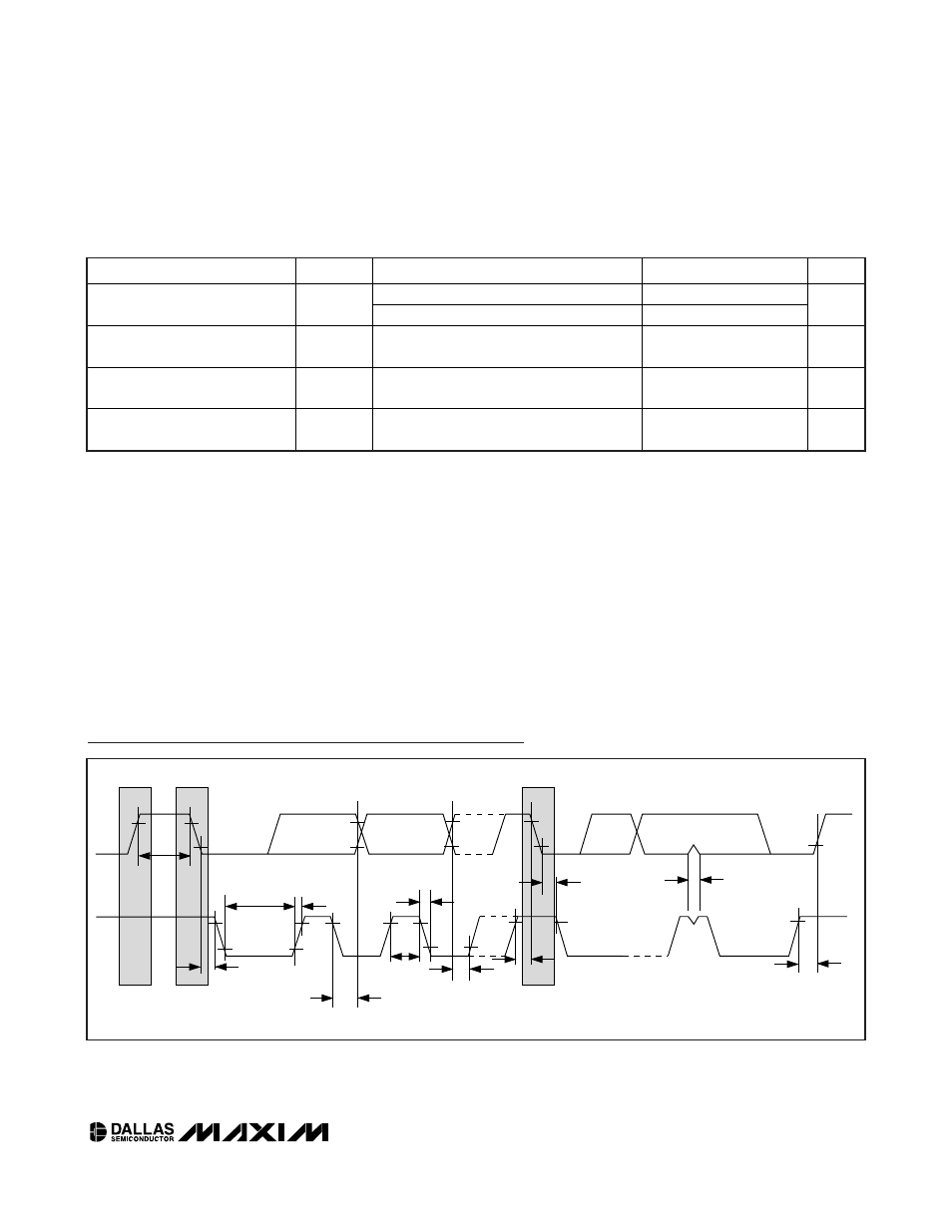
Data Transfer on I
2
C Serial Bus
SDA
SCL
t
HD:STA
t
LOW
t
HIGH
t
R
t
F
t
BUF
t
HD:DAT
t
SU:DAT
REPEATED
START
t
SU:STA
t
HD:STA
t
SU:STO
t
SP
STOP
START