Ac waveforms, input pin clock(1), Ac characteristics, input pin clock, Atv750b(l) – Rainbow Electronics ATV750BL User Manual
Page 6: Ac waveforms, input pin clock
6
ATV750B(L)
0301I–08/01
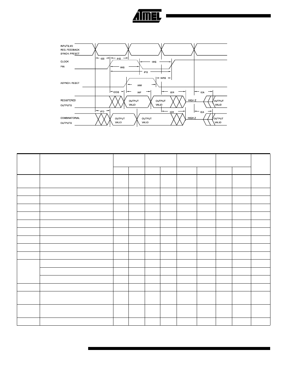
AC Waveforms, Input Pin Clock
Note:
1. Timing measurement reference is 1.5V. Input AC driving levels are 0.0V and 3.0V, unless otherwise specified.
AC Characteristics, Input Pin Clock
Symbol
Parameter
-7
-10
B/BL
-15
B/BL
-25
Units
Min
Max
Min
Max
Min
Max
Min
Max
t
PD
Input or Feedback to
Non-Registered Output
7.5
10
15
25
ns
t
EA
Input to Output Enable
7.5
10
15
25
ns
t
ER
Input to Output Disable
7.5
10
15
25
ns
t
COS
Clock to Output
0
6.5
0
7
0
10
0
12
ns
t
CFS
Clock to Feedback
0
3.5
0
5
0
5.5
0
7
ns
t
SS
Input Setup Time
4
6.5
8/12.5
9/15
ns
t
SFS
Feedback Setup Time
4
5
7
9
ns
t
HS
Hold Time
0
0
0
0
ns
t
PS
Clock Period
7
10
12
16
ns
t
WS
Clock Width
3.5
5
6
8
ns
f
MAXS
External Feedback 1/(t
SS
+t
COS
)
95
74
55/44
48/37
MHz
Internal Feedback 1/(t
SFS
+t
CFS
)
133
100
80
62
MHz
No Feedback 1/(t
PS
)
142
100
83
62
MHz
t
AW
Asynchronous Reset Width
5
10
15
20
ns
t
ARS
Asynchronous Reset
Recovery Time
5
10
15
25
ns
t
AP
Asynchronous Reset to
Registered Output Reset
8
10
15
25
ns
t
SPS
Setup Time, Synchronous Preset
5
5/9
11
15
ns