Power-up reset, Pin capacitance, Atv750b(l) – Rainbow Electronics ATV750BL User Manual
Page 10
10
ATV750B(L)
0301I–08/01
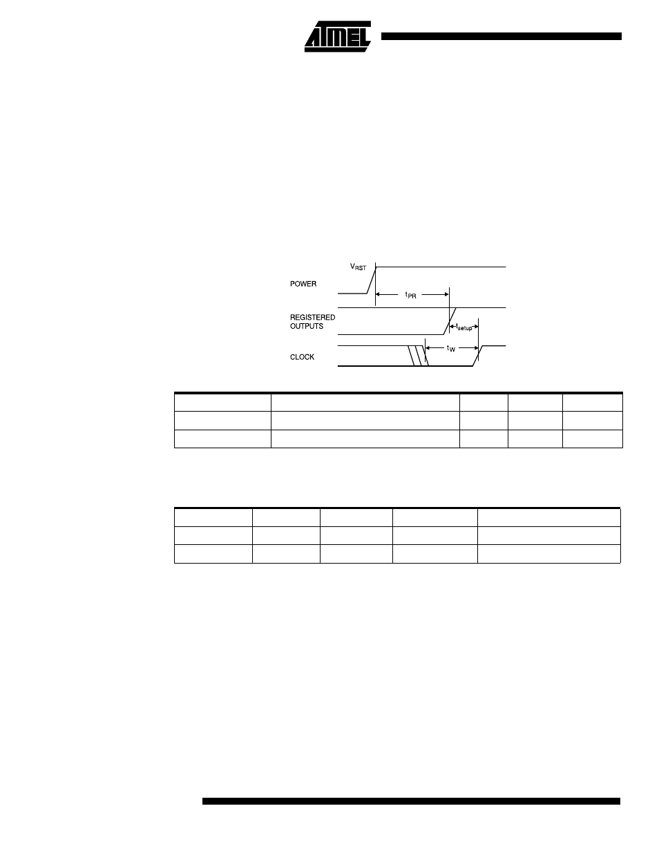
Power-up Reset
The registers in the ATV750B(L) is designed to reset during power-up. At a point delayed
slightly from V
CC
crossing V
RST
, all registers will be reset to the low state. The output state will
depend on the polarity of the output buffer.
This feature is critical for state machine initialization. However, due to the asynchronous
nature of reset and the uncertainty of how V
CC
actually rises in the system, the following condi-
tions are required:
1.
The V
CC
rise must be monotonic,
2.
After reset occurs, all input and feedback setup times must be met before driving the
clock terms or pin high, and
3.
The clock pin, or signals from which clock terms are derived, must remain stable during
t
PR
.
Parameter
Description
Typ
Max
Units
t
PR
Power-up Reset Time
600
1000
ns
V
RST
Power-up Reset Voltage
3.8
4.5
V
Pin Capacitance
f = 1 MHz, T = 25°C
(1)
Typ
Max
Units
Conditions
C
IN
5
8
pF
V
IN
= 0V
C
OUT
6
8
pF
V
OUT
= 0V