Rainbow Electronics DS2890 User Manual
Page 6
DS2890
6 of 28
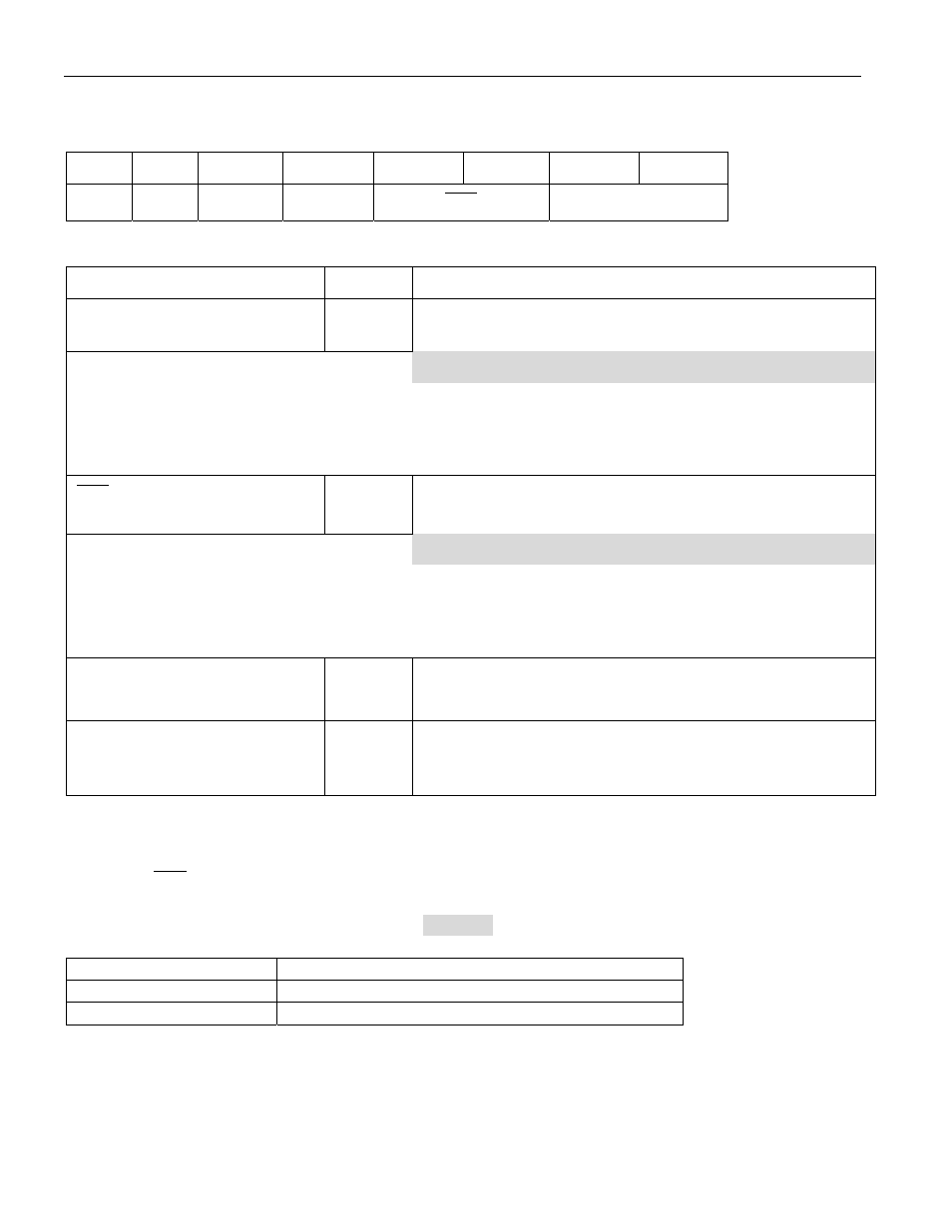
FIGURE 4. POTENTIOMETER CONTROL REGISTER
Control Register Bit Encoding
b7
b6
b5
b4
b3
b2
b1
b0
X
CPC
X
X
WN
WN
Control Register Bit Definitions*
Description
Bit(s)
Definition
WN: wiper number to control
b1..b0
2 bit binary value representing the potentiometer wiper to
control:
If 00b: potentiometer 1 wiper
If 01b: potentiometer 2 wiper
If 10b: potentiometer 3 wiper
If 11b: potentiometer 4 wiper
WN : inverted wiper number to
control
b3..b2
1’s complement of potentiometer wiper to control:
If 11b: potentiometer 1 wiper
If 10b: potentiometer 2 wiper
If 01b: potentiometer 3 wiper
If 00b: potentiometer 4 wiper
If 0: the charge pump is OFF
CPC: charge pump control
b6
If 1: the charge pump is ON
X: don’t care.
b4,b5,b7
These bits are reserved for future use by Dallas
Semiconductor. These bits should be written to a value of
0.
*Note:
Control Register power-on defaults: Charge Pump is OFF (CPC=0), Wiper Number to control is wiper #1
(WN=00b, WN =11b).
Valid DS2890 control values are highlighted:
value
Thus for the DS2890, valid control register values are:
Control Register Value
Description
00001100b
charge pump off, potentiometer #1 wiper selected
01001100b
charge pump on, potentiometer #1 wiper selected
As shown in Figure 22 and discussed in the “POTENTIOMETER FUNCTION COMMANDS” section,
no change in device state will occur if an invalid control register value is sent.