Pin description functional diagram, Detailed description – Rainbow Electronics MAX15054 User Manual
Page 6
High-Side MOSFET Driver for HB LED Drivers
and DC-DC Applications
MAX15054
6 ______________________________________________________________________________________
Pin Description
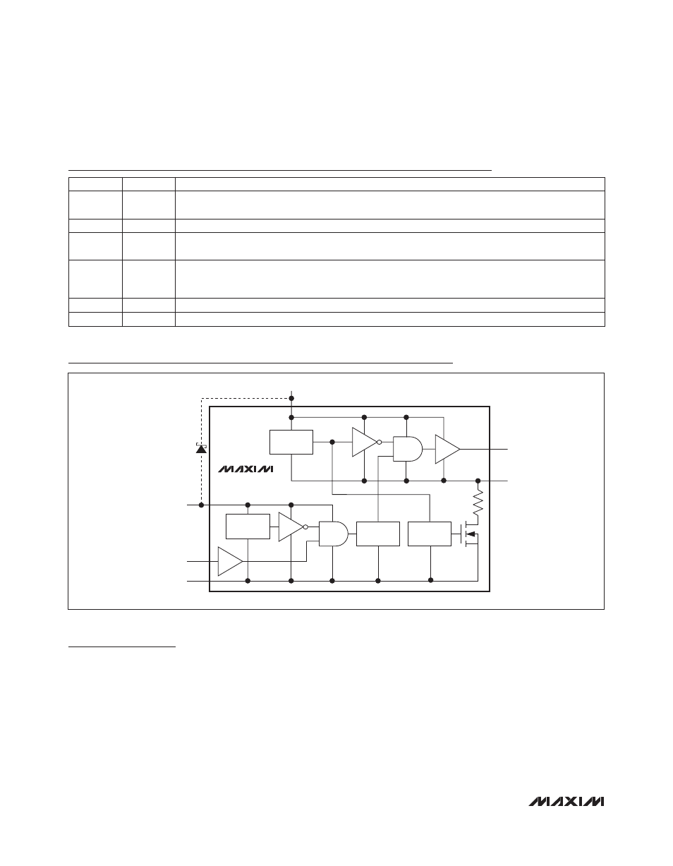
Functional Diagram
Detailed Description
The MAX15054 n-channel MOSFET driver controls an
external high-side MOSFET in high-voltage, high-current
applications. This driver operates with a supply voltage of
4.6V to 5.5V, and consumes only 300FA of supply current
during typical switching operations (f
SW
= 500kHz) and
no-load conditions. The MAX15054 provides 2.5A (typ)
sink
/
source peak current and is capable of operating with
large capacitive loads and with switching frequencies
up to 2MHz. The device is used to drive the high-side
MOSFET without requiring an isolation device such as an
optocoupler or a drive transformer.
The high-side driver is controlled by a CMOS logic
referenced to ground and is powered by a bootstrap
circuit formed by an external diode and capacitor.
Undervoltage lockout (UVLO) protection is provided for
both the high- and low-side driver supplies (BST and
V
DD
) and includes a UVLO hysteresis of 0.2V (typ).
The MAX15054’s fast switching times and very short
propagation delays (11ns, typ) are ideal for high-
frequency applications. Internal logic circuitry prevents
shoot-through during output state changes and minimizes
package power dissipation.
LOW-SIDE
UVLO
HDRV
LX
V
DD
BST
D
1
EXTERNAL
HI
GND
LEVEL
SHIFT UP
HIGH-SIDE
UVLO
LEVEL SHIFT
DOWN
MAX15054
PIN
NAME
FUNCTION
1
HI
5V CMOS Logic Input. HI is referenced to GND and is capable of withstanding voltages up to 13.5V for
any V
DD
voltage.
2
GND
Ground
3
V
DD
Input Supply Voltage. Valid supply voltage ranges from 4.6V to 5.5V. Bypass V
DD
to GND with a 0.1FF
ceramic capacitor as close as possible to the device.
4
BST
Boost Flying Capacitor Connection. Connect a minimum of a 0.1FF ceramic capacitor between BST
and LX for the high-side MOSFET driver supply. Connect a bootstrap Schottky diode between V
DD
and BST.
5
HDRV
High-Side Gate-Driver Output. Driver output to drive the high-side external MOSFET gate.
6
LX
Source Connection for High-Side MOSFET. LX also serves as a return terminal for the high-side driver.